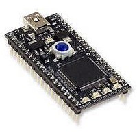
OM11042,598 NXP Semiconductors, OM11042,598 Datasheet - Page 9

OM11042,598
Manufacturer Part Number
OM11042,598
Description
Microcontroller Modules & Accessories mbed LPC2368 Demo Board
Manufacturer
NXP Semiconductors
Datasheet
1.OM11042598.pdf
(59 pages)
Specifications of OM11042,598
Product
Microcontroller Modules
Data Bus Width
32 bit
Core Processor
LPC2368
Clock Speed
60 MHz
Interface Type
Ethernet, CAN, I2C, SPI, UART
Operating Supply Voltage
3 V to 3.6 V
Lead Free Status / RoHS Status
Lead free / RoHS Compliant
NXP Semiconductors
Table 4.
LPC2364_65_66_67_68_6
Product data sheet
Symbol
P0[6]/
I2SRX_SDA/
SSEL1/MAT2[0]
P0[7]/
I2STX_CLK/
SCK1/MAT2[1]
P0[8]/
I2STX_WS/
MISO1/MAT2[2]
P0[9]/
I2STX_SDA/
MOSI1/MAT2[3]
P0[10]/TXD2/
SDA2/MAT3[0]
P0[11]/RXD2/
SCL2/MAT3[1]
P0[15]/TXD1/
SCK0/SCK
P0[16]/RXD1/
SSEL0/SSEL
P0[17]/CTS1/
MISO0/MISO
Pin description
Pin
79
78
77
76
48
49
62
63
61
[1]
[1]
[1]
[1]
[1]
[1]
[1]
[1]
[1]
…continued
Ball
B8
A9
C8
A10
H7
K9
F10
F8
F9
[1]
[1]
[1]
[1]
[1]
[1]
[1]
[1]
[1]
Type
I/O
I/O
I/O
O
I/O
I/O
I/O
O
I/O
I/O
I/O
O
I/O
I/O
I/O
O
I/O
O
I/O
O
I/O
I
I/O
O
I/O
O
I/O
I/O
I/O
I
I/O
I/O
I/O
I
I/O
I/O
Description
P0[6] — General purpose digital input/output pin.
I2SRX_SDA — Receive data. It is driven by the transmitter and read by the
receiver. Corresponds to the signal SD in the I
SSEL1 — Slave Select for SSP1.
MAT2[0] — Match output for Timer 2, channel 0.
P0[7] — General purpose digital input/output pin.
I2STX_CLK — Transmit Clock. It is driven by the master and received by
the slave. Corresponds to the signal SCK in the I
SCK1 — Serial Clock for SSP1.
MAT2[1] — Match output for Timer 2, channel 1.
P0[8] — General purpose digital input/output pin.
I2STX_WS — Transmit Word Select. It is driven by the master and
received by the slave. Corresponds to the signal WS in the I
specification.
MISO1 — Master In Slave Out for SSP1.
MAT2[2] — Match output for Timer 2, channel 2.
P0[9] — General purpose digital input/output pin.
I2STX_SDA — Transmit data. It is driven by the transmitter and read by the
receiver. Corresponds to the signal SD in the I
MOSI1 — Master Out Slave In for SSP1.
MAT2[3] — Match output for Timer 2, channel 3.
P0[10] — General purpose digital input/output pin.
TXD2 — Transmitter output for UART2.
SDA2 — I
MAT3[0] — Match output for Timer 3, channel 0.
P0[11] — General purpose digital input/output pin.
RXD2 — Receiver input for UART2.
SCL2 — I
MAT3[1] — Match output for Timer 3, channel 1.
P0[15] — General purpose digital input/output pin.
TXD1 — Transmitter output for UART1.
SCK0 — Serial clock for SSP0.
SCK — Serial clock for SPI.
P0[16] — General purpose digital input/output pin.
RXD1 — Receiver input for UART1.
SSEL0 — Slave Select for SSP0.
SSEL — Slave Select for SPI.
P0[17] — General purpose digital input/output pin.
CTS1 — Clear to Send input for UART1.
MISO0 — Master In Slave Out for SSP0.
MISO — Master In Slave Out for SPI.
Rev. 06 — 1 February 2010
2
2
C2 clock input/output (this is not an open-drain pin).
C2 data input/output (this is not an open-drain pin).
LPC2364/65/66/67/68
Single-chip 16-bit/32-bit microcontrollers
2
2
S-bus specification.
S-bus specification.
2
S-bus specification.
© NXP B.V. 2010. All rights reserved.
2
S-bus
9 of 59


