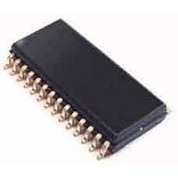
CS8427-CZZ Cirrus Logic Inc, CS8427-CZZ Datasheet - Page 16

CS8427-CZZ
Manufacturer Part Number
CS8427-CZZ
Description
Audio DSPs 96 kHz Digital Audio Transceiver
Manufacturer
Cirrus Logic Inc
Datasheet
1.CS8427-DZZ.pdf
(60 pages)
Specifications of CS8427-CZZ
Operating Supply Voltage
4.5 V to 5.5 V
Supply Current
6.3 mA to 76.6 mA
Operating Temperature Range
- 10 C to + 70 C
Mounting Style
SMD/SMT
Input Voltage
4.8 V to 5.8 V
Package / Case
TSSOP-28
Rohs Compliant
Yes
Supply Voltage Range
4.5V To 5.5V
Logic Case Style
TSSOP
No. Of Pins
28
Supply Voltage Max
5.5V
Supply Voltage Min
4.5V
Lead Free Status / RoHS Status
Lead free / RoHS Compliant
Available stocks
Company
Part Number
Manufacturer
Quantity
Price
Company:
Part Number:
CS8427-CZZ
Manufacturer:
CIRRUS
Quantity:
67
Part Number:
CS8427-CZZ
Manufacturer:
CIRRUS
Quantity:
20 000
6. AES3 RECEIVER
The CS8427 includes an AES3 digital audio re-
ceiver and an AES3 digital audio transmitter. A
comprehensive
read/write access to the channel status and user
data. This buffering scheme is described in
pendix B: Channel Status and User Data Buffer
Management”.
The AES3 receiver accepts and decodes audio
and digital data according to the AES3, IEC60958
(S/PDIF), and EIAJ CP-1201 interface standards.
The receiver consists of a differential input stage,
accessed through pins RXP and RXN, a PLL
based clock recovery circuit, and a decoder which
separates the audio data from the channel status
and user data.
External components are used to terminate and
isolate the incoming data cables from the CS8427.
These components are detailed in
External AES3/SPDIF/IEC60958 Transmitter and
Receiver Components” on page
6.1
A special mode is available that allows the clock
that is being input through the OMCK pin to be out-
put through the RMCK pin. This feature is con-
trolled by the SWCLK bit in control register 1.
When the PLL loses lock, the frequency of the
VCO drops to 300 kHz. The SWCLK function al-
lows the clock from RMCK to be used as a clock in
the system without any disruption when input is re-
moved from the Receiver. This clock switching is
performed glitch free. None of the internal circuitry
that is clocked from the PLL is driven by the OMCK
being output from RMCK. This function is available
only in software mode.
6.2
Please see Appendix C for general description of
the PLL, selection of recommended PLL filter com-
ponents, and layout considerations. Figure 5
shows the recommended configuration of the two
capacitors and one resistor that comprise the PLL
filter.
16
OMCK System Clock Mode
PLL, Jitter Attenuation, and
Varispeed
buffering
scheme
50.
“Appendix A:
provides
“Ap-
6.3
While decoding the incoming AES3 data stream,
the CS8427 can identify several kinds of error, in-
dicated in the Receiver Error register. The UN-
LOCK bit indicates whether the PLL is locked to
the incoming AES3 data. The V bit reflects the cur-
rent validity bit status. The BIP (bi-phase) error bit
indicates an error in incoming bi-phase coding.
The PAR (parity) bit indicates a received parity er-
ror.
The error bits are “sticky”: they are set on the first
occurrence of the associated error and will remain
set until the user reads the register through the
control port. This enables the register to log all un-
masked errors that occurred since the last time the
register was read.
The Receiver Error Mask register allows masking
of individual errors. The bits in this register serve
as masks for the corresponding bits of the Receiv-
er Error Register. If a mask bit is set to 1, the error
is unmasked, which implies the following: its occur-
rence will be reported in the receiver error register,
induce a pulse on RERR, invoke the occurrence of
a RERR interrupt, and affect the current audio
sample according to the status of the HOLD bits.
The HOLD bits allow a choice of holding the previ-
ous sample, replacing the current sample with zero
(mute), or not changing the current audio sample.
If a mask bit is set to 0, the error is masked, which
implies the following: its occurrence will not be re-
ported in the receiver error register, will not induce
a pulse on RERR or generate a RERR interrupt,
and will not affect the current audio sample. The
QCRC and CCRC errors do not affect the current
audio sample, even if unmasked
6.4
The first two bytes of the Channel Status block are
decoded into the Receiver Channel Status regis-
ter. The setting of the CHS bit in the Channel Sta-
tus Data Buffer Control register determines
whether the channel status decodes are from the A
channel (CHS = 0) or B channel (CHS = 1).
The PRO (professional) bit is extracted directly.
For consumer data, the COPY (copyright) bit is ex-
tracted, and the category code and L bits are de-
coded to determine SCMS status, indicated by the
ORIG (original) bit. If the category code is set to
Error Reporting and Hold Function
Channel Status Data Handling
CS8427
DS477F5


