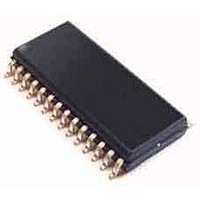
CS8427-CZZ Cirrus Logic Inc, CS8427-CZZ Datasheet - Page 25

CS8427-CZZ
Manufacturer Part Number
CS8427-CZZ
Description
Audio DSPs 96 kHz Digital Audio Transceiver
Manufacturer
Cirrus Logic Inc
Datasheet
1.CS8427-DZZ.pdf
(60 pages)
Specifications of CS8427-CZZ
Operating Supply Voltage
4.5 V to 5.5 V
Supply Current
6.3 mA to 76.6 mA
Operating Temperature Range
- 10 C to + 70 C
Mounting Style
SMD/SMT
Input Voltage
4.8 V to 5.8 V
Package / Case
TSSOP-28
Rohs Compliant
Yes
Supply Voltage Range
4.5V To 5.5V
Logic Case Style
TSSOP
No. Of Pins
28
Supply Voltage Max
5.5V
Supply Voltage Min
4.5V
Lead Free Status / RoHS Status
Lead free / RoHS Compliant
Available stocks
Company
Part Number
Manufacturer
Quantity
Price
Company:
Part Number:
CS8427-CZZ
Manufacturer:
CIRRUS
Quantity:
67
Part Number:
CS8427-CZZ
Manufacturer:
CIRRUS
Quantity:
20 000
9. CONTROL PORT DESCRIPTION AND
The control port is used to access the registers, al-
lowing the CS8427 to be configured for the desired
operational modes and formats. In addition, Chan-
nel Status and User data may be read and written
through the control port. The operation of the con-
trol port may be completely asynchronous with re-
spect to the audio sample rates. However, to avoid
potential interference problems, the control port
pins should remain static if no operation is re-
quired.
The control port has two modes: SPI and I²C, with
the CS8427 acting as a slave device. SPI mode is
selected if there is a high to low transition on the
AD0/CS pin after the RST pin has been brought
high. I²C mode is selected by connecting the
AD0/CS pin to VL+ or DGND, thereby permanently
selecting the desired AD0 bit address state.
9.1
In SPI mode, CS is the CS8427 chip select signal;
CCLK is the control port bit clock (input into the
CS8427 from the microcontroller); CDIN is the in-
put data line from the microcontroller; CDOUT is
the output data line to the microcontroller. Data is
clocked in on the rising edge of CCLK and out on
the falling edge.
Figure 17
SPI mode. To write to a register, bring CS low. The
first seven bits on CDIN form the chip address and
must be 0010000b. The eighth bit is a read/write
indicator (R/W), which should be low to write. The
next eight bits form the Memory Address Pointer
(MAP), which is set to the address of the register
that is to be updated. The next eight bits are the
data which will be placed into the register designat-
ed by the MAP. During writes, the CDOUT output
stays in the Hi-Z state. It may be externally pulled
high or low with a 47 kΩ resistor, if desired.
There is a MAP auto increment capability, enabled
by the INCR bit in the MAP register. If INCR is a ze-
ro, the MAP will stay constant for successive read
or writes. If INCR is set to a 1, then the MAP will au-
toincrement after each byte is read or written, al-
lowing block reads or writes of successive
registers.
DS477F5
TIMING
SPI
shows the operation of the control port in
TM
Mode
To read a register, the MAP has to be set to the
correct address by executing a partial write cycle
which finishes (CS high) immediately after the
MAP byte. The MAP auto increment bit (INCR)
may be set or not, as desired. To begin a read,
bring CS low, send out the chip address, and set
the read/write bit (R/W) high. The next falling edge
of CCLK will clock out the MSB of the addressed
register (CDOUT will leave the high impedance
state). If the MAP auto increment bit is set to 1, the
data for successive registers will appear consecu-
tively.
9.2
In I²C mode, SDA is a bidirectional data line. Data
is clocked into and out of the part by SCL, with the
clock to data relationship as shown in
There is no CS pin. Each individual CS8427 is giv-
en a unique address. Pins AD0 and AD1 form the
two least significant bits of the chip address and
should be connected to VL+ or DGND as desired.
The EMPH pin is used to set the AD2 bit, by con-
necting a resistor from the EMPH pin to VL+ or to
DGND. The state of the pin is sensed while the
CS8427 is being reset. The upper four bits of the
seven bit address field are fixed at 0010b. To com-
municate with a CS8427, the chip address field,
which is the first byte sent to the CS8427, should
be 0010b followed by the settings of the EMPH,
AD1, and AD0. The eighth bit of the address is the
R/W bit. If the operation is a write, the next byte is
the Memory Address Pointer (MAP) which selects
the register to be read or written. If the operation is
a read, the contents of the register pointed to by
the MAP will be output. Setting the auto increment
bit in MAP allows successive reads or writes of
consecutive registers. Each byte is separated by
an acknowledge bit, ACK, which is output from the
CS8427 after each input byte is read. The ACK bit
is input to the CS8427 from the microcontroller af-
ter each transmitted byte. I²C mode is supported
only with VL+ = 5.0 V.
9.3
The CS8427 has a comprehensive interrupt capa-
bility. The INT output pin is intended to drive the in-
terrupt input pin on the host microcontroller. The
INT pin may be set to be active low, active high, or
active low with no active pull-up transistor. This last
I²C Mode
Interrupts
CS8427
Figure
18.
25


