PUMB2,115 NXP Semiconductors, PUMB2,115 Datasheet - Page 2
PUMB2,115
Manufacturer Part Number
PUMB2,115
Description
Digital Transistors / Resistor Biased TRNS DOUBL RET TAPE7
Manufacturer
NXP Semiconductors
Series
-r
Datasheet
1.PUMB2115.pdf
(8 pages)
Specifications of PUMB2,115
Configuration
Dual
Transistor Polarity
PNP
Typical Input Resistor
47 KOhm
Typical Resistor Ratio
1
Mounting Style
SMD/SMT
Package / Case
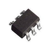
SOT-363
Collector- Emitter Voltage Vceo Max
50 V
Peak Dc Collector Current
100 mA
Maximum Operating Temperature
+ 150 C
Minimum Operating Temperature
- 65 C
Power - Max
300mW
Current - Collector (ic) (max)
100mA
Voltage - Collector Emitter Breakdown (max)
50V
Transistor Type
2 PNP - Pre-Biased (Dual)
Current - Collector Cutoff (max)
1µA
Dc Current Gain (hfe) (min) @ Ic, Vce
80 @ 5mA, 5V
Vce Saturation (max) @ Ib, Ic
150mV @ 500µA, 10mA
Resistor - Base (r1) (ohms)
47K
Resistor - Emitter Base (r2) (ohms)
47K
Frequency - Transition
-
Mounting Type
Surface Mount
Lead Free Status / RoHS Status
Lead free / RoHS Compliant
Frequency - Transition
-
Lead Free Status / Rohs Status
Lead free / RoHS Compliant
Other names
934055443115 PUMB2 T/R


NXP Semiconductors
FEATURES
• Built-in bias resistors
• Simplified circuit design
• Reduction of component count
• Reduced pick and place costs.
APPLICATIONS
• Low current peripheral drivers
• Replacement of general purpose transistors in digital
• Control of IC inputs.
DESCRIPTION
PNP/PNP resistor-equipped transistors (see “Simplified
outline, symbol and pinning” for package details).
PRODUCT OVERVIEW
Note
1. * = p: Made in Hong Kong.
SIMPLIFIED OUTLINE, SYMBOL AND PINNING
2003 Oct 15
PEMB2
PUMB2
PEMB2
PUMB2
TYPE NUMBER
TYPE NUMBER
applications
PNP/PNP resistor-equipped transistors;
R1 = 47 kΩ, R2 = 47 kΩ
* = t: Made in Malaysia.
* = W: Made in China.
PHILIPS
SOT666
SOT363
Top view
PACKAGE
6
1
SIMPLIFIED OUTLINE AND SYMBOL
5
2
SC-88
EIAJ
−
3
4
MAM477
2
MARKING CODE
TR1
QUICK REFERENCE DATA
V
I
TR1
TR2
R1
R2
SYMBOL
O
6
1
CEO
B*2
B2
(1)
R1
R2
5
2
R2
R1
collector-emitter
voltage
output current (DC)
PNP
PNP
bias resistor
bias resistor
PARAMETER
PEMD12
PUMD12
4
3
TR2
COMPLEMENT
NPN/PNP
PEMB2; PUMB2
PIN
1
2
3
4
5
6
−
−
−
−
47
47
TYP.
Product data sheet
PEMH2
PUMH2
PINNING
COMPLEMENT
emitter TR1
base TR1
collector TR2
emitter TR2
base TR2
collector TR1
DESCRIPTION
NPN/NPN
−50
−100
−
−
−
−
MAX.
V
mA
−
−
kΩ
kΩ
UNIT
Related parts for PUMB2,115
Image
Part Number
Description
Manufacturer
Datasheet
Request
R


Part Number:
Description:
Digital Transistors TRNS DOUBL RET TAPE7
Manufacturer:
NXP Semiconductors
Datasheet:

Part Number:
Description:
NXP Semiconductors designed the LPC2420/2460 microcontroller around a 16-bit/32-bitARM7TDMI-S CPU core with real-time debug interfaces that include both JTAG andembedded trace
Manufacturer:
NXP Semiconductors
Datasheet:

Part Number:
Description:
NXP Semiconductors designed the LPC2458 microcontroller around a 16-bit/32-bitARM7TDMI-S CPU core with real-time debug interfaces that include both JTAG andembedded trace
Manufacturer:
NXP Semiconductors
Datasheet:
Part Number:
Description:
NXP Semiconductors designed the LPC2468 microcontroller around a 16-bit/32-bitARM7TDMI-S CPU core with real-time debug interfaces that include both JTAG andembedded trace
Manufacturer:
NXP Semiconductors
Datasheet:
Part Number:
Description:
NXP Semiconductors designed the LPC2470 microcontroller, powered by theARM7TDMI-S core, to be a highly integrated microcontroller for a wide range ofapplications that require advanced communications and high quality graphic displays
Manufacturer:
NXP Semiconductors
Datasheet:
Part Number:
Description:
NXP Semiconductors designed the LPC2478 microcontroller, powered by theARM7TDMI-S core, to be a highly integrated microcontroller for a wide range ofapplications that require advanced communications and high quality graphic displays
Manufacturer:
NXP Semiconductors
Datasheet:
Part Number:
Description:
The Philips Semiconductors XA (eXtended Architecture) family of 16-bit single-chip microcontrollers is powerful enough to easily handle the requirements of high performance embedded applications, yet inexpensive enough to compete in the market for hi
Manufacturer:
NXP Semiconductors
Datasheet:
Part Number:
Description:
The XA-S3 device is a member of Philips Semiconductors? XA(eXtended Architecture) family of high performance 16-bitsingle-chip microcontrollers
Manufacturer:
NXP Semiconductors
Datasheet:

Part Number:
Description:
The NXP BlueStreak LH75401/LH75411 family consists of two low-cost 16/32-bit System-on-Chip (SoC) devices
Manufacturer:
NXP Semiconductors
Datasheet:
Part Number:
Description:
The NXP LPC3130/3131 combine an 180 MHz ARM926EJ-S CPU core, high-speed USB2
Manufacturer:
NXP Semiconductors
Datasheet:
Part Number:
Description:
The NXP LPC3141 combine a 270 MHz ARM926EJ-S CPU core, High-speed USB 2
Manufacturer:
NXP Semiconductors
Part Number:
Description:
The NXP LPC3143 combine a 270 MHz ARM926EJ-S CPU core, High-speed USB 2
Manufacturer:
NXP Semiconductors

Part Number:
Description:
The NXP LPC3152 combines an 180 MHz ARM926EJ-S CPU core, High-speed USB 2
Manufacturer:
NXP Semiconductors