DN2535N5-G Supertex, DN2535N5-G Datasheet
DN2535N5-G
Specifications of DN2535N5-G
Available stocks


Related parts for DN2535N5-G


DN2535N5-G Summary of contents
Page 1
... MOS devices. Characteristic of all MOS structures, this device is free from thermal runaway and thermally-induced secondary breakdown. Supertex’s vertical DMOS FETs are ideally suited to a wide range of switching and amplifying applications where high breakdown voltage, high input impedance, low input capacitance, and fast switching speeds are desired ...
Page 2
... DS(ON) DS(ON) G Forward transconductance FS C Input capacitance ISS C Common source output capacitance OSS C Reverse transfer capacitance RSS Supertex inc. Package may or may not include the following marks Code for week sealed DN5DW = “Green” Packaging TO-243AA (SOT-89) (N8) I Power Dissipation D (pulsed ...
Page 3
... Notes: 1. All D.C. parameters 100% tested All A.C. parameters sample tested. Switching Waveforms and Test Circuit 0V INPUT 10% -10V t (ON d(ON) r VDD 10% OUTPUT 0V 90% Supertex inc. (cont.) Min Typ - - - - - - - - - - - 800 C unless otherwise stated. (Pulse test: 300µs pulse, 2% duty cycle.) O 90% t (OFF) ...
Page 4
... V = 10V DS 0.4 0.3 0.2 0 100 I (Milliamps) D Maximum Rated Safe Operating Area 1 TO-92/TO-220 (pulsed TO-243AA (DC) 0.1 TO-92 (DC) 0. 0.001 (Volts) DS Supertex inc. 250 V = 1.0V GS 0.5V 200 0V 150 100 -0.5V -1.0V 240 320 400 125 150 200 250 1.0 TO-220 (DC) 0.8 0.6 0.4 ...
Page 5
... Transfer Characteristics 0. 10V DS 0.32 0.24 0.16 0. (Volts) GS Capacitance Vs. Drain-to-Source Voltage 200 C ISS 150 100 C OSS 50 C RSS (Volts) DS Supertex inc. (cont.) 150 100 125 10V ● 1235 Bordeaux Drive, Sunnyvale, CA 94089 5 On-Resistance vs. Drain Current 100 160 240 320 ...
Page 6
... Bottom View Symbol A MIN .170 Dimensions NOM - (inches) MAX .210 JEDEC Registration TO-92. * This dimension is not specified in the JEDEC drawing. † This dimension differs from the JEDEC drawing. Drawings not to scale. Supertex Doc.#: DSPD-3TO92N3, Version E041009. Supertex inc Front View ...
Page 7
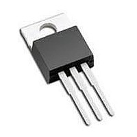
... MAX .190 .055 .120 † JEDEC Registration TO-220, Variation AB, Issue K, April 2002. * This dimension is not specified in the JEDEC drawing. † This dimension differs from the JEDEC drawing. Drawings not to scale. Supertex Doc. #: DSPD-3TO220N5, Version C041009. Supertex inc. A Φ Side View ...
Page 8
... JEDEC Registration TO-243, Variation AA, Issue C, July 1986. † This dimension differs from the JEDEC drawing Drawings not to scale. Supertex Doc. #: DSPD-3TO243AAN8, Version E051509. (The package drawing(s) in this data sheet may not reflect the most current specifications. For the latest package outline information go to http://www.supertex.com/packaging.html.) does not recommend the use of its products in life support applications, and will not knowingly sell them for use in such applications unless it receives Supertex inc ...