VN3205N8-G Supertex, VN3205N8-G Datasheet

MOSFET Small Signal 50V 0.3Ohm

VN3205N8-G

Manufacturer Part Number
VN3205N8-G
Description
MOSFET Small Signal 50V 0.3Ohm
Manufacturer
Supertex
Datasheet

Specifications of VN3205N8-G

Minimum Operating Temperature
- 55 C
Configuration
Single
Transistor Polarity
N-Channel
Resistance Drain-source Rds (on)
0.3 Ohm @ 10 V
Drain-source Breakdown Voltage
50 V
Gate-source Breakdown Voltage
+/- 20 V
Continuous Drain Current
1.5 A
Power Dissipation
1600 mW
Maximum Operating Temperature
+ 150 C
Mounting Style
SMD/SMT
Package / Case
SOT-89
Lead Free Status / RoHS Status
Lead free / RoHS Compliant
Absolute Maximum Ratings
Features
Applications
-G indicates package is RoHS compliant (‘Green’)
* MIL visual screening available.
Absolute Maximum Ratings are those values beyond which damage to the device
may occur. Functional operation under these conditions is not implied. Continuous
operation of the device at the absolute rating level may affect device reliability. All
voltages are referenced to device ground.
*
Ordering Information
Parameter
Drain-to-source voltage
Drain-to-gate voltage
Gate-to-source voltage
Operating and storage temperature
Soldering temperature*
VN3205
Distance of 1.6mm from case for 10 seconds.
Device
Free from secondary breakdown
Low power drive requirement
Ease of paralleling
Low C
Excellent thermal stability
Integral source-drain diode
High input impedance and high gain
Motor controls
Converters
Amplifiers
Switches
Power supply circuits
Drivers (relays, hammers, solenoids, lamps,
memories, displays, bipolar transistors, etc.)
ISS
and fast switching speeds
VN3205N3-G
TO-92
VN3205P-G
14-Lead
N-Channel Enhancement-Mode
Vertical DMOS FETs
1235 Bordeaux Drive, Sunnyvale, CA 94089
PDIP
Package Options
-55°C to +150°C
VN3205N8-G
+300°C
TO-243AA
(SOT-89)
Value
BV
BV
±20V
DGS
DSS
General Description
This enhancement-mode (normally-off) transistor utilizes a
vertical DMOS structure and Supertex’s well-proven silicon-gate
manufacturing process. This combination produces a device with
the power handling capabilities of bipolar transistors and with
the high input impedance and positive temperature coefficient
inherent in MOS devices. Characteristic of all MOS structures,
this device is free from thermal runaway and thermally induced
secondary breakdown.
Supertex’s vertical DMOS FETs are ideally suited to a wide range
of switching and amplifying applications where high breakdown
voltage, high input impedance, low input capacitance, and fast
switching speeds are desired.
Pin Configurations
VN3205ND
SOURCE
TO-92 (N3)
Die*
Tel: 408-222-8888
DRAIN
D4
G4
GATE
14-Lead PDIP (P)
S4
BV
N/C
D1
DSS
G1
(V)
50
S3
/BV
S1
G3
www.supertex.com
DGS
TO-243AA (SOT-89) (N8)
D3
N/C
S2
DRAIN
G2
R
D2
max
DS(ON)
0.3
(Ω)
GATE
VN3205
DRAIN
SOURCE
V
max
2.4
GS(th)
(V)

Related parts for VN3205N8-G

VN3205N8-G Summary of contents

Page 1

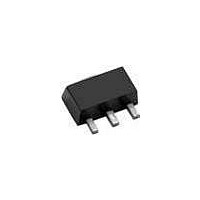
... Supertex’s vertical DMOS FETs are ideally suited to a wide range of switching and amplifying applications where high breakdown voltage, high input impedance, low input capacitance, and fast switching speeds are desired. Package Options 14-Lead TO-243AA PDIP (SOT-89) VN3205N8-G VN3205ND Pin Configurations Value BV DSS BV DGS ±20V -55° ...

Page 2

... Max Rating 0.8 Max Rating 10V 0. 4.5V 0. 4.5V Ω 10V 0 10V 0.85 1 10V 1.5 - mho V = 25V ● Tel: 408-222-8888 ● www.supertex.com VN3205 I I † DR DRM (A) (A) 1.2 8.0 1.5 8.0 1.5 8.0 = 10mA 10mA 10mA 125 5. 1. 0.75A 2.0A D ...

Page 3

... C unless otherwise stated. (Pulse test: 300µs pulse, 2% duty cycle.) O 90% t (OFF d(OFF) f 10% 90% 1235 Bordeaux Drive, Sunnyvale, CA 94089 3 Max Units Conditions 300 120 25V 1.0MHz 25V 2.0A 10Ω GEN - PULSE GENERATOR R GEN INPUT ● Tel: 408-222-8888 ● www.supertex.com VN3205 = 1. 1. OUTPUT D.U.T. ...

Page 4

... Power Dissipation vs. Case Temperature 3.2 P-DIP 2.8 2.4 2.0 TO-243AA ( T = 25° 1.6 1.2 TO-92 0.8 0 100 125 Thermal Response Characteristics 1.0 0.8 TO-243AA 0 25° 1.6W D 0.4 0.2 TO- 25° 0.001 0.01 0.1 1.0 t (seconds) p ● Tel: 408-222-8888 ● www.supertex.com VN3205 GS 10V 150 10 ...

Page 5

... Bordeaux Drive, Sunnyvale, CA 94089 5 On-Resistance vs. Drain Current 10V (amperes and R Variation with Temperature (th 10V, 3A DS(ON 1mA GS(th) - 100 Gate Drive Dynamic Characteristics 10V 40V DS 6 325 215 (nanocoulombs) G ● Tel: 408-222-8888 ● www.supertex.com VN3205 20 1.6 1.4 1.2 1.0 0.8 0.6 150 5 ...

Page 6

... Seating Plane E1 1 Symbol A MIN .170 Dimensions NOM - (inches) MAX .210 JEDEC Registration TO-92. * This dimension is not specified in the JEDEC drawing. † This dimension differs from the JEDEC drawing. Drawings not to scale. Supertex Doc.#: DSPD-3TO92N3, Version E041009 Front View Bottom View ...

Page 7

... TO-243AA (SOT-89) Package Outline (N8) b Symbol A b MIN 1.40 0.44 Dimensions NOM - (mm) MAX 1.60 0.56 JEDEC Registration TO-243, Variation AA, Issue C, July 1986. † This dimension differs from the JEDEC drawing Drawings not to scale. Supertex Doc. #: DSPD-3TO243AAN8, Version E051509 0.36 0.35 4.40 1. 0.48 0.44 4.60 1.83 ● ...

Page 8

... Supertex inc. does not recommend the use of its products in life support applications, and will not knowingly sell them for use in such applications unless it receives an adequate “product liability indemnification insurance agreement.” Supertex inc. does not assume responsibility for use of devices described, and limits its liability to the replacement of the devices determined defective due to workmanship ...

Related keywords