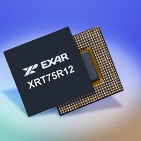
XRT75R12IB-F Exar Corporation, XRT75R12IB-F Datasheet - Page 2

XRT75R12IB-F
Manufacturer Part Number
XRT75R12IB-F
Description
Peripheral Drivers & Components (PCIs) 12 Channel 3.3V-5V temp -45 to 85C
Manufacturer
Exar Corporation
Datasheet
1.XRT75R12IB-F.pdf
(90 pages)
Specifications of XRT75R12IB-F
Maximum Operating Temperature
+ 85 C
Minimum Operating Temperature
- 40 C
Mounting Style
SMD/SMT
Operating Supply Voltage
3.3 V
Package / Case
TBGA-420
Ic Interface Type
Parallel, Serial
Supply Voltage Range
3.135V To 3.465V
Operating Temperature Range
-40°C To +85°C
Digital Ic Case Style
BGA
No. Of Pins
420
Filter Terminals
SMD
Rohs Compliant
Yes
Data Rate Max
51.84Mbps
Lead Free Status / RoHS Status
Lead free / RoHS Compliant
XRT75R12
TWELVE CHANNEL E3/DS3/STS-1 LINE INTERFACE UNIT WITH JITTER ATTENUATOR
FEATURES
RECEIVER
TRANSMITTER
JITTER ATTENUATOR
CONTROL AND DIAGNOSTICS
R
Redundancy)
On chip Clock and Data Recovery circuit for high
input jitter tolerance
Meets E3/DS3/STS-1 Jitter Tolerance Requirement
Detects and Clears LOS as per G.775
Receiver Monitor mode handles up to 20 dB flat
loss with 6 dB cable attenuation
On chip B3ZS/HDB3 encoder and decoder that can
be either enabled or disabled
On-chip clock synthesizer provides the appropriate
rate clock from a single 12.288 MHz Clock
Provides low jitter output clock
R
Redundancy)
Compliant with Bellcore GR-499, GR-253 and ANSI
T1.102 Specification for transmit pulse
Tri-state Transmit output capability for redundancy
applications
Each Transmitter can be independently turned on
or off
Transmitters provide Voltage Output Drive
On chip advanced crystal-less Jitter Attenuator for
each channel
Jitter Attenuator can be selected in Receive,
Transmit path, or disabled
Meets ETSI TBR 24 Jitter Transfer Requirements
Compliant with jitter transfer template outlined in
ITU G.751, G.752, G.755 and GR-499-CORE,1995
standards
16 or 32 bits selectable FIFO size
Parallel Microprocessor Interface for control and
configuration
Supports
monitoring
3
3
Technology
Technology
optional
(Reconfigurable,
(Reconfigurable,
internal
Transmit
Relayless
Relayless
driver
2
TRANSMIT INTERFACE CHARACTERISTICS
RECEIVE INTERFACE CHARACTERISTICS
Each channel supports Analog, Remote and Digital
Loop-backs
Single 3.3 V ± 5% power supply
5 V Tolerant digital inputs
Available in 420 pin TBGA Thermally enhanced
Package
- 40°C to 85°C Industrial Temperature Range
Accepts either Single-Rail or Dual-Rail data from
Terminal Equipment and generates a bipolar signal
to the line
Integrated Pulse Shaping Circuit
Built-in B3ZS/HDB3 Encoder (which can be
disabled)
Accepts Transmit Clock with duty cycle of 30%-
70%
Generates pulses that comply with the ITU-T G.703
pulse template for E3 applications
Generates pulses that comply with the DSX-3 pulse
template, as specified in Bellcore GR-499
and ANSI T1.102_1993
Generates pulses that comply with the STSX-1
pulse template, as specified in Bellcore GR-253-
CORE
Transmitter can be turned off in order to support
redundancy designs
Integrated Adaptive Receive Equalization (optional)
for optimal Clock and Data Recovery
Declares and Clears the LOS defect per ITU-T
G.775 requirements for E3 and DS3 applications
Meets Jitter Tolerance Requirements, as specified
in ITU-T G.823_1993 for E3 Applications
Meets Jitter Tolerance Requirements, as specified
in Bellcore GR-499-CORE for DS3 Applications
Declares Loss of Lock (LOL) Alarm
Built-in B3ZS/HDB3 Decoder (which can be
disabled)
Recovered Data can be muted while the LOS
Condition is declared
Outputs either Single-Rail or Dual-Rail data to the
Terminal Equipment
REV. 1.0.4
-CORE


