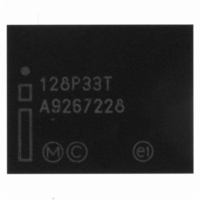
PC28F128P33T85A NUMONYX, PC28F128P33T85A Datasheet - Page 57

PC28F128P33T85A
Manufacturer Part Number
PC28F128P33T85A
Description
IC FLASH 128MBIT 85NS 64EZBGA
Manufacturer
NUMONYX
Series
StrataFlash™r
Datasheet
1.PC28F128P33T85A.pdf
(96 pages)
Specifications of PC28F128P33T85A
Format - Memory
FLASH
Memory Type
FLASH
Memory Size
128M (8Mx16)
Speed
85ns
Interface
Parallel
Voltage - Supply
2.3 V ~ 3.6 V
Operating Temperature
-40°C ~ 85°C
Package / Case
64-TBGA
Cell Type
NOR
Density
128Mb
Access Time (max)
85ns
Interface Type
Parallel/Serial
Boot Type
Top
Address Bus
23b
Operating Supply Voltage (typ)
2.5/3.3V
Operating Temp Range
-40C to 85C
Package Type
EZBGA
Sync/async
Async/Sync
Operating Temperature Classification
Industrial
Operating Supply Voltage (min)
2.3V
Operating Supply Voltage (max)
3.6V
Word Size
16b
Number Of Words
8M
Supply Current
28mA
Mounting
Surface Mount
Pin Count
64
Lead Free Status / RoHS Status
Lead free / RoHS Compliant
Other names
888065
888065
PC28F128P33T85 888065
888065
PC28F128P33T85 888065
Available stocks
Company
Part Number
Manufacturer
Quantity
Price
Company:
Part Number:
PC28F128P33T85A
Manufacturer:
Micron Technology Inc
Quantity:
10 000
Numonyx™ StrataFlash
Table 30: Device Identifier Information (Sheet 2 of 2)
Table 31: Device ID codes
11.2.4
11.3
November 2007
Order Number: 314749-05
64-bit Factory-Programmed Protection Register
64-bit User-Programmable Protection Register
Lock Register 1
128-bit User-Programmable Protection Registers
Notes:
1.
Device Code
Note:
BBA = Block Base Address.
The 512-Mbit devices do not have a Device ID associated with them. Each die within the stack can be identified by either
of the 256-Mbit Device ID codes depending on its parameter option.
CFI Query
The CFI Query command instructs the device to output Common Flash Interface (CFI)
data when read. See
on issuing the CFI Query command.
shows CFI information and address offsets within the CFI database.
Programming Operations
The device supports three programming methods: Word Programming (40h/10h),
Buffered Programming (E8h, D0h), and Buffered Enhanced Factory Programming (80h,
D0h). The following sections describe device programming in detail.
Successful programming requires the addressed block to be unlocked. If the block is
locked down, WP# must be deasserted and the block must be unlocked before
attempting to program the block. Attempting to program a locked block causes a
program error (SR[4] and SR[1] set) and termination of the operation. See
11.4.5, “Security Modes” on page 64
The Numonyx™ StrataFlash
Mbit Programming Regions. See
addressing. Execute in Place (XIP) applications must partition the memory such that
code and data are in separate programming regions. XIP is executing code directly
from flash memory. Each Programming Region should contain only code or data but not
both. The following terms define the difference between code and data. System designs
must use these definitions when partitioning their code and data for the Numonyx™
StrataFlash
ID Code Type
Code :
Data :
®
Embedded Memory (P33)
Item
Execution code ran out of the flash device on a continuous basis in the system.
Information periodically programmed into the flash device and read back (e.g. execution code
shadowed and executed in RAM, pictures, log files, etc.).
®
Embedded Memory (P33) device.
Section 9.6, “Device Command Bus Cycles” on page 44
®
Embedded Memory (P33) is segmented into multiple 8-
Device Density
Section 4.4, “Memory Maps” on page 22
128-Mbit
256-Mbit
64-Mbit
Appendix , “Common Flash Interface” on page 77
for details on locking and unlocking blocks.
0x8A–0x109
Address
0x81–0x84
0x85–0x88
0x89
(1)
(Top Parameter)
881D
881E
891F
–T
Device Identifier Codes
Factory Protection Register Data
User Protection Register Data
Protection Register Lock Data
PR-LK1
(Bottom Parameter)
Data
for complete
8820
8821
8922
Section
–B
for details
Datasheet
57


