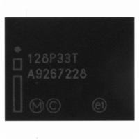
PC28F128P33T85A NUMONYX, PC28F128P33T85A Datasheet - Page 67

PC28F128P33T85A
Manufacturer Part Number
PC28F128P33T85A
Description
IC FLASH 128MBIT 85NS 64EZBGA
Manufacturer
NUMONYX
Series
StrataFlash™r
Datasheet
1.PC28F128P33T85A.pdf
(96 pages)
Specifications of PC28F128P33T85A
Format - Memory
FLASH
Memory Type
FLASH
Memory Size
128M (8Mx16)
Speed
85ns
Interface
Parallel
Voltage - Supply
2.3 V ~ 3.6 V
Operating Temperature
-40°C ~ 85°C
Package / Case
64-TBGA
Cell Type
NOR
Density
128Mb
Access Time (max)
85ns
Interface Type
Parallel/Serial
Boot Type
Top
Address Bus
23b
Operating Supply Voltage (typ)
2.5/3.3V
Operating Temp Range
-40C to 85C
Package Type
EZBGA
Sync/async
Async/Sync
Operating Temperature Classification
Industrial
Operating Supply Voltage (min)
2.3V
Operating Supply Voltage (max)
3.6V
Word Size
16b
Number Of Words
8M
Supply Current
28mA
Mounting
Surface Mount
Pin Count
64
Lead Free Status / RoHS Status
Lead free / RoHS Compliant
Other names
888065
888065
PC28F128P33T85 888065
888065
PC28F128P33T85 888065
Available stocks
Company
Part Number
Manufacturer
Quantity
Price
Company:
Part Number:
PC28F128P33T85A
Manufacturer:
Micron Technology Inc
Quantity:
10 000
Numonyx™ StrataFlash
.
Figure 32: Protection Register Map
11.4.8.1
November 2007
Order Number: 314749-05
The first 128-bit Protection Register is comprised of two 64-bit (8-word) segments. The
lower 64-bit segment is pre-programmed at the Numonyx factory with a unique 64-bit
number. The other 64-bit segment, as well as the other sixteen 128-bit Protection
Registers, are blank. Users can program these registers as needed. When programmed,
users can then lock the Protection Register(s) to prevent additional bit programming
(see
The user-programmable Protection Registers contain one-time programmable (OTP)
bits; when programmed, PR bits cannot be erased. Each Protection Register can be
accessed multiple times to program individual bits, as long as the register remains
unlocked.
Each Protection Register has an associated Lock Register bit. When a Lock Register bit
is programmed, the associated Protection Register can only be read; it can no longer be
programmed. Additionally, because the Lock Register bits themselves are OTP, when
programmed, Lock Register bits cannot be erased. Therefore, when a Protection
Register is locked, it cannot be unlocked.
Reading the Protection Registers
The Protection Registers can be read from any address. To read the Protection Register,
first issue the Read Device Identifier command at any address to place the device in the
Read Device Identifier state (see
Figure 32, “Protection Register Map” on page
®
Embedded Memory (P33)
0x109
0x102
0x8A
0x91
0x89
0x88
0x85
0x84
0x81
0x80
15 14 13 12 11 10 9
15 14 13 12 11 10 9
128-bit Protection Register 16
128-bit Protection Register 1
128-Bit Protection Register 0
(Factory-Programmed)
(User-Programmable)
(User-Programmable)
(User-Programmable)
Lock Register 1
64-bit Segment
64-bit Segment
Lock Register 0
8
8
Section 9.6, “Device Command Bus Cycles” on
7
7
6
6
5
5
4
4
3
3
2
2
1
1
0
0
67).
Datasheet
67


