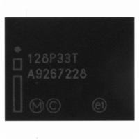
PC28F128P33T85A NUMONYX, PC28F128P33T85A Datasheet - Page 71

PC28F128P33T85A
Manufacturer Part Number
PC28F128P33T85A
Description
IC FLASH 128MBIT 85NS 64EZBGA
Manufacturer
NUMONYX
Series
StrataFlash™r
Datasheet
1.PC28F128P33T85A.pdf
(96 pages)
Specifications of PC28F128P33T85A
Format - Memory
FLASH
Memory Type
FLASH
Memory Size
128M (8Mx16)
Speed
85ns
Interface
Parallel
Voltage - Supply
2.3 V ~ 3.6 V
Operating Temperature
-40°C ~ 85°C
Package / Case
64-TBGA
Cell Type
NOR
Density
128Mb
Access Time (max)
85ns
Interface Type
Parallel/Serial
Boot Type
Top
Address Bus
23b
Operating Supply Voltage (typ)
2.5/3.3V
Operating Temp Range
-40C to 85C
Package Type
EZBGA
Sync/async
Async/Sync
Operating Temperature Classification
Industrial
Operating Supply Voltage (min)
2.3V
Operating Supply Voltage (max)
3.6V
Word Size
16b
Number Of Words
8M
Supply Current
28mA
Mounting
Surface Mount
Pin Count
64
Lead Free Status / RoHS Status
Lead free / RoHS Compliant
Other names
888065
888065
PC28F128P33T85 888065
888065
PC28F128P33T85 888065
Available stocks
Company
Part Number
Manufacturer
Quantity
Price
Company:
Part Number:
PC28F128P33T85A
Manufacturer:
Micron Technology Inc
Quantity:
10 000
Numonyx™ StrataFlash
Figure 35: Buffer Program Flowchart
November 2007
Order Number: 314749-05
Yes
Read Status Register
Read Status Register
Issue Write to Buffer
Command E8h and
and Block Address
(at Block Address)
Write Word Count,
Write Buffer Data,
Write Confirm D0h
Program Complete
Is WSM Ready?
Another Buffered
Check if Desired
Supports Buffer
Target Address
Set Timeout or
Block Address
Block Address
Programming?
Loop Counter
Start Address
Full Status
Get Next
X = N?
SR.7 =?
Writes?
SR.7 =
Device
X = 0
Start
1 = Yes
Yes
Yes
No
1
®
Embedded Memory (P33)
No
No
Write Buffer Data,
Buffered Program
Use Single Word
Write to another
Abort Bufferred
Block Address
Block Address
Programming
Program?
X = X + 1
Expired?
or Count
Timeout
Suspend
Aborted
Program
No
No
Yes
No
Yes
Yes
Suspend
Program
Loop
1. Word count values on DQ
register. Count ranges for this device are N = 0000h to 0001Fh.
2. The device outputs the status register when read.
3. Write Buffer contents will be programmed at the device start
address or destination flash address.
4. Align the start address on a Write Buffer boundary for
maximum programming performance (i.e., A
address = 0).
5. The device aborts the Buffered Program command if the
current address is outside the original block address.
6. The Status register indicates an "improper command
sequence" if the Buffered Program command is aborted. Follow
this with a Clear Status Register command.
Full status check can be done after all erase and write
sequences complete. Write FFh after the last operation to reset
the device to read array mode.
(Notes 1, 2)
(Notes 3, 4)
(Notes 5, 6)
Operation
Standby
Standby
Read
Read
Write
Write
Write
Write
Write
Bus
Command
Program
Write to
Confirm
Buffer
0
-DQ
Data = E8H
Addr = Block Address
SR.7 = Valid
Addr = Block Address
Check SR.7
1 = Device WSM is Busy
0 = Device WSM is Ready
Data = N-1 = Word Count
N = 0 corresponds to count = 1
Addr = Block Address
Data = Write Buffer Data
Addr = Start Address
Data = Write Buffer Data
Addr = Block Address
Data = D0H
Addr = Block Address
Status register Data
CE# and OE# low updates SR
Addr = Block Address
Check SR.7
1 = WSM Ready
0 = WSM Busy
7
are loaded into the Count
Comments
4
–A
0
of the start
Datasheet
71


