EVAL-ADF4001EBZ2 Analog Devices Inc, EVAL-ADF4001EBZ2 Datasheet - Page 14
EVAL-ADF4001EBZ2
Manufacturer Part Number
EVAL-ADF4001EBZ2
Description
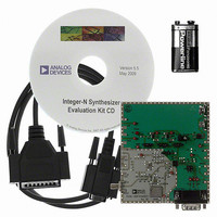
BOARD EVAL FOR ADF4001
Manufacturer
Analog Devices Inc
Datasheet
1.ADF4001BRUZ.pdf
(16 pages)
Specifications of EVAL-ADF4001EBZ2
Main Purpose
Timing, Clock Generator
Embedded
No
Utilized Ic / Part
ADF4001
Primary Attributes
1 Input, 1 Output
Secondary Attributes
2.7 V ~ 5.5 V Supply
Lead Free Status / RoHS Status
Lead free / RoHS Compliant


ADF4001
COHERENT CLOCK GENERATION
When testing A/D converters, it is often advantageous to use a
coherent test system, that is, a system that ensures a specific
relationship between the A/D converter input signal and the
A/D converter sample rate. Thus, when doing an FFT on this
data, there is no longer any need to apply the window weighting
function. Figure 8 shows how the ADF4001 can be used to handle
all the possible combinations of the input signal frequency and
sampling rate. The first ADF4001 is phase locked to a VCO. The
output of the VCO is also fed into the N divider of the second
ADF4001. This results in both ADF4001s being coherent with
the REF
MUXOUT signal of the second ADF4001 is coherent with the f
frequency to the ADC. This is used as f
TRI-BAND CLOCK GENERATION CIRCUIT
In multiband applications, it is necessary to realize different
clocks from one master clock frequency. For example, GSM
uses a 13 MHz system clock, WCDMA uses 19.44 MHz, and
CDMA uses 19.2 MHz. The circuit in Figure 9 shows how to
use the ADF4001 to generate GSM, WCDMA, and CDMA
system clocks from a single 52 MHz master clock. The low RF
f
low as
clock frequencies can be realized using the formula
SHUTDOWN CIRCUIT
The circuit in Figure 10 shows how to shut down both the
ADF4001 and the accompanying VCO. The ADG702 switch
goes open circuit when a Logic 1 is applied to the IN input.
The low cost switch is available in both SOT-23 and micro
SOIC packages.
MIN
MODEL 1051
BRUEL &
KJAER
SQUARE
OUTPUT
OUTPUT
specification and the ability to program R and N values as
SINE
IN
1 makes the ADF4001 suitable for this. Other f
. Since the REF
REF
Figure 8. Coherent Clock Generator
IN
ADF4001
ADF4001
f
R1
f
OUT
S
= (f
IN
=
IN
REF
N1)/(R1
comes from the signal generator, the
N1
N2
IN
×
N2)
RF
RF
MUXOUT
CP
(
N
IN
IN
RF
S
, the sampling clock.
÷
FILTER
LOOP
R
f
IN
)
NC7S04
A
100MHz
IN
SAMPLING
VCO
CLOCK
CONVERTER
f
S
UNDER
TEST
OUT
A/D
IN
–14–
FREF
MASTER
CLOCK
52MHz
IN
7
CPGND
AV
V
Figure 10. Local Oscillator Shutdown Circuit
Figure 9. Tri-Band System Clock Generation
DD
DD
REF
REF
REF
3
ADF4001
15
DV
IN
IN
IN
DD
AGND
16
4
V
V
ADF4001
ADF4001
R2
1300
ADF4001
P
486
P
N2
POWER-DOWN CONTROL
24
65
R3
N3
R1
4
1
N1
DGND
RF
RF
CE
R
SET
IN
10
CP
IN
9
A
B
6
5
1
2
100pF
DECOUPLING CAPACITORS AND INTERFACE
SIGNALS HAVE BEEN OMITTED FROM THE
DIAGRAM IN THE INTEREST OF GREATER CLARITY.
FILTER
100pF
10k
LOOP
CP
RF
CP
RF
CP
RF
IN
IN
IN
RF
RF
RF
FILTER
FILTER
FILTER
LOOP
LOOP
LOOP
IN
51
ADG702
V
GND
CC
S
D
VCXO
VCO
OR
19.44MHz
19.2MHz
GND
13MHz
V
VCXO
VCXO
VCXO
DD
100pF
CLOCK FOR WCDMA
CLOCK FOR CDMA
19.44MHz SYSTEM
CLOCK FOR GSM
19.2MHz SYSTEM
13MHz SYSTEM
100pF
18
REV. A
18
18
RF
OUT
Related parts for EVAL-ADF4001EBZ2
Image
Part Number
Description
Manufacturer
Datasheet
Request
R

Part Number:
Description:
IC, ADJ LDO REG, 1.5V TO 5V 250mA MSOP-8
Manufacturer:
Vishay
Datasheet:

Part Number:
Description:
IC, ADJ LDO REG, 1.5V TO 5V 0.6A 8-TSSOP
Manufacturer:
Vishay
Datasheet:
Part Number:
Description:
IC, ADJ LDO REG, 1.5V TO 5V 250mA MSOP-8
Manufacturer:
Vishay
Datasheet:

Part Number:
Description:
IC ADJ LDO REG 1.5V TO 5V 150mA 5-SOT-23
Manufacturer:
Vishay
Datasheet:

Part Number:
Description:
BOARD EVAL AS1324-AD
Manufacturer:
austriamicrosystems
Datasheet:
Part Number:
Description:
IC, ADJ LDO REG, 1.5V TO 5V 0.6A 8-TSSOP
Manufacturer:
Vishay
Datasheet:

Part Number:
Description:
IC, ADJ LDO REG, 1.5V TO 5V, 0.3A, MSOP8
Manufacturer:
Vishay
Datasheet:
Part Number:
Description:
IC, ADJ LDO REG, 1.5V TO 5V, 0.3A, MSOP8
Manufacturer:
Vishay
Datasheet:
Part Number:
Description:
IC, ADJ LDO REG 1.215V TO 5V 0.3A MSOP-8
Manufacturer:
Vishay
Datasheet:
Part Number:
Description:
IC, ADJ LDO REG 1.215V TO 5V 0.3A MSOP-8
Manufacturer:
Vishay
Datasheet:

Part Number:
Description:
±1.7g Dual-Axis IMEMS Accelerometer Evaluation Board
Manufacturer:
Analog Devices Inc
Datasheet:

Part Number:
Description:
IC MULTIPLIER ANALOG 8-SOIC T/R
Manufacturer:
Analog Devices Inc
Datasheet:

Part Number:
Description:
IC ANALOG MULTIPLIER 8-DIP
Manufacturer:
Analog Devices Inc
Datasheet:
Part Number:
Description:
IC ANALOG MULTIPLIER 8-SOIC
Manufacturer:
Analog Devices Inc
Datasheet:
Part Number:
Description:
IC ANALOG MULTIPLIER 8-DIP
Manufacturer:
Analog Devices Inc
Datasheet: