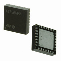
AIS326DQTR STMicroelectronics, AIS326DQTR Datasheet
AIS326DQTR
Specifications of AIS326DQTR


Related parts for AIS326DQTR


AIS326DQTR Summary of contents
Page 1
... The sensing element, capable of detecting the acceleration, is manufactured using a dedicated Table 1. Device summary Operating temperature Order code AIS326DQ AIS326DQTR June 2010 3-axis, low g accelerometer with digital output process developed produce inertial sensors and actuators in silicon. The IC interface instead is manufactured using a CMOS process that allows high level of ...
Page 2
Contents Contents 1 Block diagram and pin description . . . . . . . . . . . . . . . . . . . . . . . . . . . . . 8 1.1 Block ...
Page 3
AIS326DQ 7.3 OFFSET_Y (17h ...
Page 4
Contents 8.3 Mechanical characteristics at 105 ° 8.4 Mechanical characteristics derived ...
Page 5
AIS326DQ List of tables Table 1. Device summary . . . . . . . . . . . . . . . . . . . . . . . . . . . . . . . . ...
Page 6
List of tables Table 49. FF_WU_THS_H register ...
Page 7
AIS326DQ List of figures Figure 1. Block diagram . . . . . . . . . . . . . . . . . . . . . . . . . . . . . . . . ...
Page 8
Block diagram and pin description 1 Block diagram and pin description 1.1 Block diagram Figure 1. Block diagram a SELF TEST 1.2 QFPN-28 pin description Figure 2. Pin connection Z DIRECTIONS OF THE DETECTABLE ACCELERATIONS 8/ CHARGE Z+ ...
Page 9
AIS326DQ Table 2. Pin description Pin 14 Name NC Internally not connected GND 0 V supply Vdd Power ...
Page 10
Mechanical and electrical specifications 2 Mechanical and electrical specifications 2.1 Mechanical characteristics Table 3. Mechanical characteristics @ Vdd = 3 -40 °C to 105 °C unless otherwise (1) noted Symbol Parameter FS Measurement range Dres Device resolution ...
Page 11
AIS326DQ Table 3. Mechanical characteristics @ Vdd = 3 -40 °C to 105 °C unless otherwise (1) noted (continued) Symbol Parameter V Self-test output change st (9) BW System bandwidth T Operating temperature range OP Wh Product ...
Page 12
Mechanical and electrical specifications 2.2 Electrical characteristics Table 4. Electrical characteristics @ Vdd=3 -40 °C to 105 °C unless otherwise noted Symbol Parameter Vdd Supply voltage Vdd_IO I/O pads supply voltage Idd Supply current Current consumption IddPdn ...
Page 13
AIS326DQ 2.3 Communication interface characteristics 2.3.1 SPI - serial peripheral interface Subject to general operating conditions for Vdd and T Table 5. SPI slave timing values Symbol tc(SPC) fc(SPC) tsu(CS) th(CS) tsu(SI) th(SI) tv(SO) th(SO) tdis(SO) 1. Values are guaranteed ...
Page 14
Mechanical and electrical specifications 2.4 Absolute maximum ratings Stresses above those listed as “absolute maximum ratings” may cause permanent damage to the device. This is a stress rating only and functional operation of the device under these conditions is not ...
Page 15
AIS326DQ 2.5 Terminology 2.5.1 Sensitivity Sensitivity describes the gain of the sensor and can be determined e.g. by applying 1 g acceleration to it. As the sensor can measure DC accelerations this can be done easily by pointing the axis ...
Page 16
Functionality 3 Functionality The AIS326DQ is a high performance, low-power, digital output 3-axes linear accelerometer packaged in a QFN package. The complete device includes a sensing element and an IC interface able to take the information from the sensing element ...
Page 17
AIS326DQ 3.3 Factory calibration The IC interface is factory calibrated for sensitivity (So) and Zero-g level (Off). The trimming values are stored inside the device by a non volatile structure. Any time the device is turned on, the trimming parameters ...
Page 18
Application hints 4 Application hints Figure 4. AIS326DQ electrical connection 10uF 100nF Vdd GND The device core is supplied through Vdd line while the I/O pads are supplied through Vdd_IO line. Power supply decoupling capacitors (100 nF ceramic, 10 µF ...
Page 19
AIS326DQ 5 Digital interface The registers embedded inside the AIS326DQ may be accessed through SPI serial interface. The latter may be SW configured to operate either in 3-wire or 4-wire interface mode. Table 7. Serial interface pin description Pin name ...
Page 20
Digital interface of CS while the last bit (bit 15, bit 23, ...) starts at the last falling edge of SPC just before the rising edge of CS. bit 0: RW bit. When 0, the data DI(7:0) is written into ...
Page 21
AIS326DQ Figure 7. Multiple bytes SPI read protocol (2 bytes example) CS SPC SDI RW MS SDO 5.1.2 SPI Write Figure 8. SPI Write protocol CS SPC SDI The SPI Write command is performed with 16 clock pulses. Multiple byte ...
Page 22
Digital interface 5.1.3 SPI Read in 3-wires mode 3-wires mode is entered by setting to ‘1’ bit SIM (SPI serial interface mode selection) in CTRL_REG2. Figure 10. SPI read protocol in 3-wires mode CS SPC SDI/O The SPI read command ...
Page 23
AIS326DQ 6 Register mapping The table given below provides a listing of the 8 bit registers embedded in the device and the related address. Table 8. Registers address map Register name WHO_AM_I OFFSET_X OFFSET_Y OFFSET_Z GAIN_X GAIN_Y GAIN_Z CTRL_REG1 CTRL_REG2 ...
Page 24
Register mapping Table 8. Registers address map (continued) Register name FF_WU_THS_H FF_WU_DURATION rw DD_CFG DD_SRC DD_ACK DD_THSI_L DD_THSI_H DD_THSE_L DD_THSE_H Registers marked as Reserved must not be changed. The writing to those registers may cause permanent damages to the device. ...
Page 25
AIS326DQ 7 Register description The device contains a set of registers which are used to control its behavior and to retrieve acceleration data. The registers necessary to change their value for normal device operation. 7.1 WHO_AM_I (0Fh) Table 9. Register ...
Page 26
Register description 7.4 OFFSET_Z (18h) Table 15. OFFSET_Z register OZ7 OZ6 Table 16. OFFSET_Z register description OZ7, OZ0 Digital offset trimming for Z-Axis 7.5 GAIN_X (19h) Table 17. GAIN_X register GX7 GX6 Table 18. GAIN_X register description GX7, GX0 Digital ...
Page 27
AIS326DQ 7.8 CTRL_REG1 (20h) Table 23. CTRL_REG1 register PD1 PD0 Table 24. CTRL_REG1 register description Power down control PD1, PD0 (00: power-down mode; 01, 10, 11: device on) Decimation factor control DF1, DF0 (00: decimate by 512; 01: decimate by ...
Page 28
Register description Table 26. CTRL_REG2 register description Full scale selection FS (0: ± ±6 g) Block data update BDU (0: continuous update; 1: output registers not updated between MSB and LSB reading) Big/little endian selection BLE (0: little ...
Page 29
AIS326DQ DRDY bit is used to enable Data-Ready (RDY/INT) pin activation. If DRDY bit is ‘0’ (default value) on Data-Ready pad a ‘0’ value is present Data-Ready signal is desired it is necessary to set to ‘1’ DRDY ...
Page 30
Register description CFS1, CFS0 bits defines the coefficient Hpc to be used to calculate the -3dB cut-off frequency of the high pass filter: 7.11 HP_FILTER_RESET (23h) Dummy register. Reading at this address zeroes instantaneously the content of the internal high ...
Page 31
AIS326DQ In big endian mode (bit BLE in CTRL_REG2 set to ‘1’) the content of this register is the MSB acceleration data and depends on bit DAS in CTRL_REG2 register as described in the following section. 7.14 OUTX_H (29h) Table ...
Page 32
Register description When reading the register in “12 bit right justified” mode the most significant bits (15:12) are replaced with bit 11 (i.e. YD15-YD12=YD11, YD11, YD11, YD11). In big endian mode (bit BLE in CTRL_REG2 set to ‘1’) the content ...
Page 33
AIS326DQ 7.19 FF_WU_CFG (30h) Table 43. FF_WU_CFG register AOI LIR Table 44. FF_WU_CFG register description And/Or combination of Interrupt events. Default value: 0. AOI (0: OR combination of interrupt events; 1: AND combination of interrupt events) Latch interrupt request. Default ...
Page 34
Register description 7.20 FF_WU_SRC (31h) Table 45. FF_WU_SRC register X IA Table 46. FF_WU_SRC register description Interrupt Active. Default value (0: no interrupt has been generated; 1: one or more interrupt events have been generated) Z High. Default ...
Page 35
AIS326DQ Table 50. FF_WU_THS_H register description THS15, THS8 Free-fall / inertial wake up acceleration threshold MSB Doc ID 14956 Rev 4 Register description 35/51 ...
Page 36
Register description 7.24 FF_WU_DURATION (36h) Table 51. FF_WU_DURATION register FWD7 FWD6 Table 52. FF_WU_DURATION register description FWD7, FWD0 This register sets the minimum duration of the free-fall/wake-up event to be recognized. 7.25 DD_CFG (38h) Table 53. DD_CFG register IEND LIR ...
Page 37
AIS326DQ Table 54. DD_CFG register description (continued) Enable interrupt generation on Y low event. Default value: 0 YLIE (0: disable interrupt request; 1: enable interrupt request on measured accel. value lower than preset threshold) Enable interrupt generation on X high ...
Page 38
Register description Direction detector source register. 7.27 DD_ACK (3Ah) Dummy register. If LIR bit in DD_CFG register is set to ‘1’, a reading at this address refreshes the DD_SRC register. Read data is not significant. 7.28 DD_THSI_L (3Ch) Table 57. ...
Page 39
AIS326DQ Table 64. DD_THSE_H register description THSE15, THSE8 Direction detection external threshold MSB Doc ID 14956 Rev 4 Register description 39/51 ...
Page 40
Typical performance characteristics 8 Typical performance characteristics 8.1 Mechanical characteristics at 25 °C Figure 11. X-axis zero-g level at 3 −80 −60 −40 −20 0 Zero−g Level Offset [mg] ...
Page 41
AIS326DQ 8.2 Mechanical characteristics at -40 °C Figure 17. X-axis zero-g level at 3 −80 −60 −40 −20 0 Zero−g Level Offset [mg] Figure 19. Y-axis zero-g level at 3.3 ...
Page 42
Typical performance characteristics 8.3 Mechanical characteristics at 105 °C Figure 23. X-axis zero-g level at 3 −100 −80 −60 −40 −20 0 Zero−g Level Offset [mg] Figure 25. Y-axis zero-g level at 3.3 ...
Page 43
AIS326DQ 8.4 Mechanical characteristics derived from measurement in the -40 °C to +105 °C temperature range Figure 29. X-axis zero-g level change vs. temperature at 3.3 V 100 −20 −40 −60 −80 −100 −50 −25 ...
Page 44
Typical performance characteristics 8.5 Electro-mechanical characteristics at 25 °C Figure 35. X and Y axes zero-g level as function of supply voltage −20 −40 −60 −80 3 3.1 3.2 3.3 Vdd [V] Figure 37. Z ...
Page 45
AIS326DQ 8.6 Electrical characteristics at 25 °C Figure 39. Current consumption in power- down mode (Vdd=3 −2 − Current consumption [uA] 8.7 Electrical characteristics at -40 °C Figure 41. ...
Page 46
Soldering information 9 Soldering information The QFPN-28 package is compliant with the ECOPACK It is qualified for soldering heat resistance according to JEDEC J-STD-020C, in MSL3 condition. Land pattern and soldering recommendations are also available at www.st.com/. 9.1 General guidelines ...
Page 47
AIS326DQ 9.2.1 PCB design rules Figure 45. Recommended land and solder mask design for QFPN packages Clearance from PCB land edge to solder mask opening ≤ 0 ensure that some solder mask remains between PCB ...
Page 48
Soldering information 9.4 Process consideration ● In case of use of no self-cleaning solder paste it is mandatory proper washing of the board after soldering to eliminate any possible source of leakage between adjacent pads due to flux residues ● ...
Page 49
AIS326DQ 10 Package information In order to meet environmental requirements, ST offers these devices in different grades of ® ECOPACK packages, depending on their level of environmental compliance. ECOPACK specifications, grade definitions and product status are available at: www.st.com. ® ...
Page 50
Revision history 11 Revision history Table 65. Document revision history Date 20-Aug-2008 04-Dec-2008 30-Apr-2010 01-Jun-2010 50/51 Revision 1 Initial release. Table 3 2 Updated Section 4: Application 3 Updated Content reworked on cover page to improve readability, ...
Page 51
... AIS326DQ Information in this document is provided solely in connection with ST products. STMicroelectronics NV and its subsidiaries (“ST”) reserve the right to make changes, corrections, modifications or improvements, to this document, and the products and services described herein at any time, without notice. All ST products are sold pursuant to ST’s terms and conditions of sale. ...