AD2S99APZ Analog Devices Inc, AD2S99APZ Datasheet - Page 4
AD2S99APZ
Manufacturer Part Number
AD2S99APZ
Description
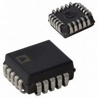
IC, PROG OSCILLATOR, 20KHZ, 5.25V, LCC20
Manufacturer
Analog Devices Inc
Type
Oscillator, Sinusoidalr
Datasheet
1.AD2S99APZ.pdf
(8 pages)
Specifications of AD2S99APZ
Supply Voltage Range
± 4.75V To ± 5.25V
Digital Ic Case Style
LCC
No. Of Pins
20
Operating Temperature Range
-40°C To +85°C
Frequency Max
20kHz
Termination Type
SMD
Frequency
20kHz
Voltage - Supply
±4.75 V ~ 5.25 V
Current - Supply
8mA
Operating Temperature
-40°C ~ 85°C
Package / Case
20-PLCC
Filter Terminals
SMD
Rohs Compliant
Yes
Accuracy
5
Lead Free Status / RoHS Status
Lead free / RoHS Compliant
Count
-
Lead Free Status / RoHS Status
Lead free / RoHS Compliant, Lead free / RoHS Compliant
Available stocks
Company
Part Number
Manufacturer
Quantity
Price
Company:

Part Number:
AD2S99APZ
Manufacturer:
AD
Quantity:
5 530
Company:
Part Number:
AD2S99APZ
Manufacturer:
AD
Quantity:
1 000
Company:
Part Number:
AD2S99APZ
Manufacturer:
Analog Devices Inc
Quantity:
135
Company:
Part Number:
AD2S99APZ
Manufacturer:
Analog Devices Inc
Quantity:
10 000
Part Number:
AD2S99APZ
Manufacturer:
ADI/亚德诺
Quantity:
20 000


AD2S99
CONNECTING THE AD2S99 OSCILLATOR
Refer to Figure 1. Positive supply voltage V
nected to Pin 12 and negative supply voltage V
nected to both Pins 19 and 20. Reversal of these power supplies will
destroy the device. The appropriate voltage level for the power
supplies is 5 V dc
connected together, and Digital Ground (Pin 6) must be con-
nected to Analog Ground (Pin 16) locally at the AD2S99.
It is recommended that decoupling capacitors are connected in
parallel between V
Ground in close proximity to the AD2S99. The recommended
values for the decoupling capacitors are 100 nF (ceramic) and
4.7 F (tantalum). When multiple AD2S99s are used, separate
decoupling capacitors should be used for each AD2S99.
FREQUENCY ADJUSTMENT
The output frequency of the AD2S99 is programmable to four
standard frequencies (2, 5, 10, or 20 kHz) using the SEL1 and
SEL2 pins. The output can also be adjusted to provide interme-
diate frequencies by connecting a resistor from the FBIAS pin to
the positive supply V
V
added resistance values for various intermediate frequencies is
provided in Figure 2. The procedure for obtaining an intermedi-
ate frequency is:
1. Set the output frequency via the SEL1, SEL2 pins to the fre-
2. Connect the frequency adjust pin FBIAS to V
For example: to obtain an output frequency of 8 kHz, set the
nominal output frequency to 10 kHz by connecting SEL1 to
GND and SEL2 to V
resistor (refer to Figure 2).
. .
.
DD
V
R
quency immediately above the required intermediate frequency.
nal resistor.
DD
X
*
*
NC = NO CONNECT
R
FIXED FREQUENCIES ONLY REQUIRE A LINK.
during normal operation. A graph showing the typical
X
IS ONLY REQUIRED FOR INTERMEDIATE FREQUENCIES.
DGND
0.1 F
COS
SIN
NC
NC
4
5
6
7
8
Figure 1. Typical Configuration
3
9
DD
50k
4.7 F
10
2
AD2S99
DD
5%. Both V
and Analog Ground and V
SS
11
1
. The FBIAS pin is connected directly to
. Connect FBIAS to V
20
12 13
19
4.7 F
18
17
16
15
14
SS
EXC
EXC
AGND
NC
NC
Pins (19 and 20) must be
100nF
SEL2 = GND ]
SEL1 = V
INCREASE R
OUTPUT FREQUENCY
(SEE GRAPH)
DD
0.1 F
REF
RESOLVER
DD
100k
should be con-
SS
SS
SS
DD
V
should be con-
]
via a 6 k
SS
COS
TO AD2S80/
AD2S90 REF INPUT
SIN
X
and Analog
–5kHz MODE
TO LOWER
via an exter-
–4–
AD2S99 OSCILLATOR OUTPUT STAGE
The output of the AD2S99 oscillator consists of two sinusoidal
signals, EXC, and EXC. EXC is 180 phase advanced with re-
spect to EXC. The excitation winding of a transducer should be
connected across EXC (Pin 17) and EXC (Pin 18).
With low impedance transducers, it may be necessary to in-
crease the output current drive of the AD2S99. In such an in-
stance, an external buffer amplifier can be used to provide gain
(as needed), and additional current drive for the excitation out-
put (either EXC or EXC) of the AD2S99, providing a single
ended drive to the transducer. Refer to Figures 6, 7 and 8 for
sample buffer configurations.
The amplitude modulated SIN and COS output signals from a re-
solver should be connected as feedback signals to the AD2S99.
The SYNREF output compensates for any primary to secondary
phase errors in the resolver. These errors can degrade the accuracy
of a Resolver-to-Digital Converter (R/D Converter).
SIN, from the resolver, should be connected to the AD2S99 SIN
input and COS should be connected to the AD2S99 COS input.
The SIN Lo, COS Lo (resolver signal returns) should be con-
nected to AGND and the R/D Converter as applicable.
The synthesized reference (SYNREF) from the AD2S99 should
be connected to the reference input pin of the R/D Converter.
The SYNREF signal is a square wave at the oscillator frequency
of amplitude 3 V p-p and is phase coherent with the SIN and
COS inputs. If this signal is used to drive the reference input of
the AD2S90 R/D Converter, a coupling capacitor and resistor to
GND must be connected between the SYNREF output of the
AD2S99 and the REF input of the R/D Converter (see Figure
3). Please read the appropriate R/D Converter data sheets for
further clarification.
LOSS OF SIGNAL
During normal operation when both the SIN and COS signals
on the resolver secondary windings are connected to the
AD2S99, the LOS output pin of the AD2S99 (Pin 11) is at a
Logic Lo ( 0.7 V). If both the SIN and COS signals on the re-
solver secondary windings fall below the LOS threshold level of
the AD2S99, the LOS pin of the AD2S99 will pull up to a
Logic Hi (V
20
18
16
14
12
10
Figure 2. Typical Added Resistance Value
8
6
4
2
0
0
DD
) level.
4
RESISTOR PULLUP TO V
ADDITIONAL RESISTANCE – k
8
12
16
DD
FROM FBIAS
20
24
28
REV. B
Related parts for AD2S99APZ
Image
Part Number
Description
Manufacturer
Datasheet
Request
R

Part Number:
Description:
±1.7g Dual-Axis IMEMS Accelerometer Evaluation Board
Manufacturer:
Analog Devices Inc
Datasheet:

Part Number:
Description:
Inertial Sensor Evaluation System
Manufacturer:
Analog Devices Inc
Datasheet:
Part Number:
Description:
Manufacturer:
Analog Devices Inc
Datasheet:
Part Number:
Description:
Manufacturer:
Analog Devices Inc
Datasheet:
Part Number:
Description:
Manufacturer:
Analog Devices Inc
Datasheet:
Part Number:
Description:
Manufacturer:
Analog Devices Inc
Datasheet:
Part Number:
Description:
Manufacturer:
Analog Devices Inc
Datasheet:
Part Number:
Description:
Manufacturer:
Analog Devices Inc
Datasheet:
Part Number:
Description:
Manufacturer:
Analog Devices Inc
Datasheet:
Part Number:
Description:
Manufacturer:
Analog Devices Inc
Datasheet:
Part Number:
Description:
Manufacturer:
Analog Devices Inc
Datasheet:
Part Number:
Description:
Manufacturer:
Analog Devices Inc
Datasheet:
Part Number:
Description:
Manufacturer:
Analog Devices Inc
Datasheet: