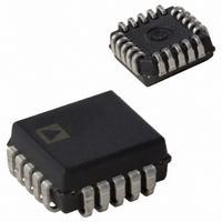
AD2S99APZ Analog Devices Inc, AD2S99APZ Datasheet - Page 7

AD2S99APZ
Manufacturer Part Number
AD2S99APZ
Description
IC, PROG OSCILLATOR, 20KHZ, 5.25V, LCC20
Manufacturer
Analog Devices Inc
Type
Oscillator, Sinusoidalr
Datasheet
1.AD2S99APZ.pdf
(8 pages)
Specifications of AD2S99APZ
Supply Voltage Range
± 4.75V To ± 5.25V
Digital Ic Case Style
LCC
No. Of Pins
20
Operating Temperature Range
-40°C To +85°C
Frequency Max
20kHz
Termination Type
SMD
Frequency
20kHz
Voltage - Supply
±4.75 V ~ 5.25 V
Current - Supply
8mA
Operating Temperature
-40°C ~ 85°C
Package / Case
20-PLCC
Filter Terminals
SMD
Rohs Compliant
Yes
Accuracy
5
Lead Free Status / RoHS Status
Lead free / RoHS Compliant
Count
-
Lead Free Status / RoHS Status
Lead free / RoHS Compliant, Lead free / RoHS Compliant
Available stocks
Company
Part Number
Manufacturer
Quantity
Price
Company:
Part Number:
AD2S99APZ
Manufacturer:
AD
Quantity:
5 530
Company:
Part Number:
AD2S99APZ
Manufacturer:
AD
Quantity:
1 000
Company:
Part Number:
AD2S99APZ
Manufacturer:
Analog Devices Inc
Quantity:
135
Company:
Part Number:
AD2S99APZ
Manufacturer:
Analog Devices Inc
Quantity:
10 000
Part Number:
AD2S99APZ
Manufacturer:
ADI/亚德诺
Quantity:
20 000
REV. B
AD2S99/AD2S93 TYPICAL CONFIGURATION
Figure 5 shows a typical circuit configuration for the AD2S99
Oscillator and the AD2S93 LVDT-to-Digital Converter. The
maximum level of the A and B transducer input signals to the
AD2S93 should be 1 V rms
nals should be star connected to the AD2S93 AGND pin. If
shielded twisted pair cables are used for the LVDT signals, the
SEL2 = GND
SEL1 = V
F
PRI
20%. All the analog ground sig-
OUT
= 5kHz
LVDT
SS
Figure 5. AD2S99 and AD2S93 Example Configuration
B
A
SEC
NC = NO CONNECT
PHASE
COMP
DGND
COS
26
27
28
1
2
3
4
SIN
NC
NC
NC
B
A
AGND
DIFF
GAIN
LOS
4
5
6
7
8
25 24
5
V
–7–
DD
3
9
R2
6
(Not to Scale)
10
AD2S99
TOP VIEW
2
(Not to Scale)
C1
shields should also be terminated at the AD2S93 AGND pin.
The SYNREF output of the AD2S99 cannot be used as the
REF input signal for the AD2S93. The zero crossing reference
for the AD2S93 should be taken from the primary winding of
the LVDT through a phase lead or lag network. The phase com-
pensation network ensures that the REF input is phase coherent
with the A and B input signals to the AD2S93.
LOS
23 22
AD2S93
TOP VIEW
7
11
1
C2
50k
8
12 13
20
0.1µF
21 20 19
19
9
10 11
18
17
16
15
14
R6
DGND
EXC
EXC
AGND
NC
NC
NULL
0.1µF
OVR
V
4.7µF
V
DIR
C3
DD
SS
18
17
16
15
14
13
12
V
DD
DMODOUT
C4
R5
R7
4.7µF
0.1µF
0.1µF
NC = NO CONNECT
V
SS
4.7µF
4.7µF
V
V
DD
SS
AD2S99


