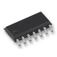
DS90LV019TM National Semiconductor, DS90LV019TM Datasheet - Page 3

DS90LV019TM
Manufacturer Part Number
DS90LV019TM
Description
LVDS PHY TRANSCEIVER 155MBS, SOIC8
Manufacturer
National Semiconductor
Datasheet
1.DS90LV019TM.pdf
(10 pages)
Specifications of DS90LV019TM
Supply Voltage Range
3V To 3.6V, 4.5V To 5.5V
Digital Ic Case Style
SOIC
No. Of Pins
14
Operating Temperature Range
-40°C To +85°C
Svhc
No SVHC (15-Dec-2010)
Operating Temperature Max
85°C
Base Number
90
Data Rate
100Mbps
Rohs Compliant
Yes
Supply Current
12mA
Driver Case Style
TSSOP
Device Type
Driver / Receiver
Filter Terminals
SMD
Data Rate Max
100Mbps
Lead Free Status / RoHS Status
Lead free / RoHS Compliant
Available stocks
Company
Part Number
Manufacturer
Quantity
Price
Company:
Part Number:
DS90LV019TM
Manufacturer:
NS
Quantity:
545
Company:
Part Number:
DS90LV019TM
Manufacturer:
LATTICE
Quantity:
1
Part Number:
DS90LV019TM
Manufacturer:
NS/国半
Quantity:
20 000
Company:
Part Number:
DS90LV019TM/NOPB
Manufacturer:
TI
Quantity:
1 500
Company:
Part Number:
DS90LV019TM/NOPB
Manufacturer:
National Semiconductor
Quantity:
1 983
Company:
Part Number:
DS90LV019TMTC
Manufacturer:
national
Quantity:
246
Part Number:
DS90LV019TMTCX
Manufacturer:
NS/国半
Quantity:
20 000
Part Number:
DS90LV019TMX
Manufacturer:
NS/国半
Quantity:
20 000
DIFFERENTIAL DRIVER CHARACTERISTICS
V
V
I
I
I
DIFFERENTIAL RECEIVER CHARACTERISTICS
V
V
I
V
V
I
DEVICE CHARACTERISTICS
V
V
I
I
V
I
I
I
I
C
C
Symbol
Symbol
DRIVER TIMING REQUIREMENTS
t
t
t
t
t
OZD
OXD
OSD
OS
IN
IH
IL
CCD
CCR
CCZ
CC
PHLD
PLHD
SKD
TLH
THL
DC Electrical Characteristics
T
V
V
Note 1: “Absolute Maximum Ratings” are these beyond which the safety of the device cannot be guaranteed. They are not meant to imply that the device should
be operated at these limits. The table of “Electrical Characteristics” provides conditions for actual device operation.
Note 2: All currents into device pins are positive; all currents out of device pins are negative. All voltages are referenced to device ground unless otherwise specified.
Note 3: All typicals are given for V
Note 4: ESD Rating:
Note 5: C
Note 6: Generator waveforms for all tests unless otherwise specified; f = 1 MHz, Z
AC Electrical Characteristics
OD
OS
OH
OL
TH
TH
IH
IL
CL
T
D output
R input
A
OD
OS
A
= −40˚C to +85˚C unless otherwise noted, V
= −40˚C to +85˚C, V
HBM (1.5 k , 100 pF)
EIAJ (0 , 200 pF)
L
includes probe and fixture capacitance.
Output Differential Voltage
V
Offset Voltage
Offset Magnitude Change
TRI-STATE Leakage
Power-Off Leakage
Output Short Circuit Current
Voltage High
Voltage Output Low
Output Short Circuit Current
Input Threshold High
Input Threshold Low
Input Current
Minimum Input High Voltage
Maximum Input Low Voltage
Input High Current
Input Low Current
Input Diode Clamp Voltage
Power Supply Current
Capacitance
Capacitance
Differential Propagation Delay High to Low
Differential Propagation Delay Low to High
Differential Skew |t
Transition Time Low to High
Transition Time High to Low
OD
Magnitude Change
>
Parameter
200V.
>
2.0 kV
CC
= 3.3V
CC
Parameter
PHLD
= +3.3V or +5.0V and T
±
− t
0.3V. (Note 6)
PLHD
|
R
V
V
V
VID = +100 mV
Inputs Open
I
V
V
0V
V
V
I
DE = RE = V
DE = RE = 0V
DE = 0V, RE = V
DE = V
OL
CLAMP
OUT
OUT
OUT
OUT
IN
IN
IN
L
CC
= 2.0 mA, VID = −100 mV
= 100
= +2.4V or 0V, V
= V
= GND or 0.4V
A
= V
= 5.5V or GND, V
= 0V, DE = V
= 0V
= 5.0
= +25˚C, unless otherwise stated.
CC
CC
= −18 mA
CC
, RE = 0V
or 2.4 V
( Figure 1 )
±
Conditions
or GND, DE = 0V
CC
0.5V. (Notes 2, 3)
R
C
( Figure 2 and Figure 3 )
CC
L
L
3
I
CC
= 100 ,
= 10 pF
OH
CC
O
Conditions
= 50 , t
= −400 µA
CC
= 5.5V or
= 0V
r
= t
f
6.0 ns (0%–100%).
DE ,RE
DO+,
DO−
R
DO+,
DO−
RI+,
D
V
RI+,
Pin
RI−
RI−
OUT
CC
IN
,
Min
2.0
1.0
0.2
0.2
−150
−100
GND
−1.5
Min
−10
−10
−10
−15
250
4.3
4.3
2.0
1
Typ
4.0
5.6
0.4
0.7
0.8
1.25
−0.8
Typ
360
−75
5.0
5.0
0.1
5.8
4.5
±
±
±
±
±
−6
12
18
6
5
5
5
1
1
1
1
1
Max
6.5
7.0
1.0
3.0
3.0
+100
Max
V
450
+10
+10
−40
+15
±
±
1.8
0.4
0.8
8.5
60
60
−4
19
48
www.national.com
8
CC
10
10
Units
Units
ns
ns
ns
ns
ns
mV
mV
mV
mA
mA
mV
mV
mA
mA
mA
mA
µA
µA
µA
µA
µA
pF
pF
V
V
V
V
V
V
V


