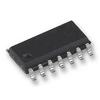
DS90LV019TM National Semiconductor, DS90LV019TM Datasheet - Page 8

DS90LV019TM
Manufacturer Part Number
DS90LV019TM
Description
LVDS PHY TRANSCEIVER 155MBS, SOIC8
Manufacturer
National Semiconductor
Datasheet
1.DS90LV019TM.pdf
(10 pages)
Specifications of DS90LV019TM
Supply Voltage Range
3V To 3.6V, 4.5V To 5.5V
Digital Ic Case Style
SOIC
No. Of Pins
14
Operating Temperature Range
-40°C To +85°C
Svhc
No SVHC (15-Dec-2010)
Operating Temperature Max
85°C
Base Number
90
Data Rate
100Mbps
Rohs Compliant
Yes
Supply Current
12mA
Driver Case Style
TSSOP
Device Type
Driver / Receiver
Filter Terminals
SMD
Data Rate Max
100Mbps
Lead Free Status / RoHS Status
Lead free / RoHS Compliant
Available stocks
Company
Part Number
Manufacturer
Quantity
Price
Company:
Part Number:
DS90LV019TM
Manufacturer:
NS
Quantity:
545
Company:
Part Number:
DS90LV019TM
Manufacturer:
LATTICE
Quantity:
1
Part Number:
DS90LV019TM
Manufacturer:
NS/国半
Quantity:
20 000
Company:
Part Number:
DS90LV019TM/NOPB
Manufacturer:
TI
Quantity:
1 500
Company:
Part Number:
DS90LV019TM/NOPB
Manufacturer:
National Semiconductor
Quantity:
1 983
Company:
Part Number:
DS90LV019TMTC
Manufacturer:
national
Quantity:
246
Part Number:
DS90LV019TMTCX
Manufacturer:
NS/国半
Quantity:
20 000
Part Number:
DS90LV019TMX
Manufacturer:
NS/国半
Quantity:
20 000
www.national.com
Applications Information
X = High or Low logic state
Z = High impedance state
L = Low state
H = High state
• Balanced cables (e.g., twisted pair) are usually better
• For cable distances
DE
H
H
H
L
than unbalanced cables (ribbon cable, simple coax) for
noise reduction and signal quality.
work effectively. For distances 0.5m
(category 3) twisted pair cable works well and is readily
available and relatively inexpensive. For distances
mended.
>
10m, and high data rates CAT 5 twisted pair is recom-
Pin Name
INPUTS
R
DO
GND
2
V
RI
D
RE
DE
OUT
CC
IN
>
±
TABLE 2. Transmitter Mode
±
&
DI
H
X
L
>
0.8
<
0.5m, most cables can be made to
11, 12
Pin #
9, 10
14
2
4
8
1
7
DO+
H
L
X
Z
FULL DUPLEX MODE
MODE SELECTED
TRI-STATE MODE
RECEIVER MODE
OUTPUTS
DRIVER MODE
(Continued)
d
Input/Output
TABLE 4. Device Pin Description
10m, CAT 3
TABLE 1. Functional Table
DO−
NA
NA
O
O
H
X
Z
L
I
I
I
I
8
TTL Driver Input
LVDS Driver Outputs
LVDS Receiver Inputs
TTL Receiver Output
Receiver Enable TTL Input (Active Low)
Driver Enable TTL Input (Active High)
Ground
Power Supply (3.3V
• There are three Fail-Safe scenarios, open input pins,
X = High or Low logic state
Z = High impedance state
L = Low state
H = High state
shorted inputs pins and terminated input pins. The first
case is guaranteed for DS90LV019. A HIGH state on
R
(one to V
Input Fail-Safe Circuit). R1 and R2 should be R
the loading to the LVDS driver . R
the impedance of the cable.
RE
H
OUT
L
L
L
DE
H
H
L
L
pin can be achieved by using two external resistors
CC
and one to GND) per Figure 10 (Terminated
100 mV
TABLE 3. Receiver Mode
±
INPUTS
Description
RE
0.3V or 5.0V
H (
L (
H
H
L
L
(RI+) − (RI−)
<
>
>
−100 mV)
+100 mV)
&
X
>
−100 mV
±
0.5V)
T
is selected to match
OUTPUT
T
H
X
L
Z
to limit


