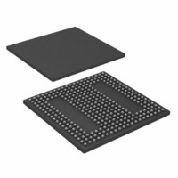
ADSP-BF538BBCZ-5F4 Analog Devices Inc, ADSP-BF538BBCZ-5F4 Datasheet - Page 48

ADSP-BF538BBCZ-5F4
Manufacturer Part Number
ADSP-BF538BBCZ-5F4
Description
IC, FLOAT-PT DSP, 16BIT, 533MHZ, BGA-316
Manufacturer
Analog Devices Inc
Series
Blackfinr
Type
Fixed Pointr
Specifications of ADSP-BF538BBCZ-5F4
No. Of Bits
16 Bit
Frequency
533MHz
Supply Voltage
1.25V
Embedded Interface Type
CAN, I2C, PPI, SPI, TWI, UART
No. Of I/o's
54
Flash Memory Size
512KB
Interface
CAN, SPI, SSP, TWI, UART
Clock Rate
533MHz
Non-volatile Memory
FLASH (512 kB)
On-chip Ram
148kB
Voltage - I/o
3.00V, 3.30V
Voltage - Core
1.25V
Operating Temperature
-40°C ~ 85°C
Mounting Type
Surface Mount
Package / Case
316-CSPBGA
Lead Free Status / RoHS Status
Lead free / RoHS Compliant
For Use With
ADZS-BFAUDIO-EZEXT - BOARD EVAL AUDIO BLACKFIN
Lead Free Status / RoHS Status
Lead free / RoHS Compliant, Lead free / RoHS Compliant
ADSP-BF538/ADSP-BF538F
TEST CONDITIONS
All timing parameters appearing in this data sheet were mea-
sured under the conditions described in this section.
shows the measurement point for ac measurements (except out-
put enable/disable). The measurement point V
V
OUTPUT
DDEXT
INPUT
OR
-
-
-
-
-
-
-
-
-
-
-
-
-
-
10
20
30
40
50
60
10
20
30
40
50
60
70
80
0
0
(nominal) = 3.0 V/3.3 V.
0
0
V
MEAS
Measurements (Except Output Enable/Disable)
Figure 42. Voltage Reference Levels for AC
0.5
Figure 41. Drive Current E (High V
Figure 40. Drive Current E (Low V
0.5
1.0
1.0
1.5
SOURCE VOLTAGE (V)
SOURCE VOLTAGE (V)
1.5
2.0
DDEXT
DDEXT
2.5
MEAS
2.0
)
)
V
V
V
V
V
MEAS
DDEXT
DDEXT
DDEXT
DDEXT
is 1.5 V for
Rev. D | Page 48 of 56 | July 2010
V
3.0
Figure 42
OL
= 2.75V
= 3.0 V
= 3.3 V
= 3.6 V
V
2.5
OL
3.5
3.0
4.0
Output Enable Time Measurement
Output pins are considered to be enabled when they have made
a transition from a high impedance state to the point when they
start driving.
The output enable time t
a reference signal reaches a high or low voltage level to the point
when the output starts driving as shown on the right side of
ure 43, “Output Enable/Disable,” on page
The time t
signal switches to when the output voltage reaches V
or V
V
when the output starts driving to when the output reaches the
V
Time t
If multiple pins (such as the data bus) are enabled, the measure-
ment value is that of the first pin to start driving.
Output Disable Time Measurement
Output pins are considered to be disabled when they stop driv-
ing, go into a high impedance state, and start to decay from their
output high or low voltage. The output disable time t
difference between t
side of
The time for the voltage on the bus to decay by ΔV is dependent
on the capacitive load C
time can be approximated by the equation:
The time t
ΔV equal to 0.5 V for V
The time t
signal switches, to when the output voltage decays ΔV from the
measured output high or output low voltage.
(MEASURED)
(MEASURED)
DDEXT
TRIP
t
DIS
TRIP
V
V
(high) or V
OH
OL
ENA
OUTPUT STOPS DRIVING
Figure
(nominal) = 3.0 V/3.3 V. Time t
(low). V
is calculated as shown in the equation:
ENA_MEASURED
DECAY
DIS_MEASURED
43.
t
TRIP
is calculated with test loads C
TRIP
DIS
REFERENCE
Figure 43. Output Enable/Disable
t
t
V
V
DIS_MEASURED
ENA
OH
(high) is 2.0 V and V
OL
(low) trip voltage.
SIGNAL
DIS_MEASURED
=
t
t
(MEASURED)
DECAY
(MEASURED) + V
DECAY
is the interval from when the reference
is the interval from when the reference
t
=
DDEXT
DIS_MEASURED
L
ENA
and the load current I
t
ENA_MEASURED
HIGH IMPEDANCE STATE
is the interval from the point when
=
(nominal) = 3.0 V/3.3 V.
(
t
and t
C
ENA
L
Δ
V
–
V
DECAY
t
) I
OUTPUT STARTS DRIVING
DECAY
–
TRIP
⁄
TRIP
t
L
48.
TRIP
as shown on the left
is the interval from
(low) is 1.0 V for
t
L
ENA_MEASURED
V
V
and I
TRIP
L
TRIP
t
. This decay
TRIP
(LOW)
V
V
(HIGH)
OH
OL
L
TRIP
DIS
, and with
(MEASURED)
(MEASURED)
is the
(high)
Fig-


