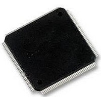
LFXP6C-5TN144C LATTICE SEMICONDUCTOR, LFXP6C-5TN144C Datasheet - Page 20

LFXP6C-5TN144C
Manufacturer Part Number
LFXP6C-5TN144C
Description
FPGA, 1.8V FLASH, INSTANT ON, SMD
Manufacturer
LATTICE SEMICONDUCTOR
Series
LatticeXPr
Datasheet
1.LFXP3C-3QN208C.pdf
(130 pages)
Specifications of LFXP6C-5TN144C
No. Of Logic Blocks
720
No. Of Macrocells
3000
Family Type
LatticeXP
No. Of Speed Grades
5
No. Of I/o's
100
Clock Management
PLL
Core Supply Voltage Range
1.71V To 3.465V
Lead Free Status / RoHS Status
Lead free / RoHS Compliant
Available stocks
Company
Part Number
Manufacturer
Quantity
Price
Company:
Part Number:
LFXP6C-5TN144C
Manufacturer:
LATTICE
Quantity:
2 291
Company:
Part Number:
LFXP6C-5TN144C
Manufacturer:
Lattice
Quantity:
60
Company:
Part Number:
LFXP6C-5TN144C
Manufacturer:
Lattice Semiconductor Corporation
Quantity:
10 000
Company:
Part Number:
LFXP6C-5TN144C-4I
Manufacturer:
LATTICE
Quantity:
2 291
Lattice Semiconductor
in selected blocks the input to the DQS delay block. If one of the bypass options is not chosen, the signal first
passes through an optional delay block. This delay, if selected, ensures no positive input-register hold-time require-
ment when using a global clock.
The input block allows two modes of operation. In the single data rate (SDR) the data is registered, by one of the
registers in the single data rate sync register block, with the system clock. In the DDR Mode two registers are used
to sample the data on the positive and negative edges of the DQS signal creating two data streams, D0 and D2.
These two data streams are synchronized with the system clock before entering the core. Further discussion on
this topic is in the DDR Memory section of this data sheet.
Figure 2-21 shows the input register waveforms for DDR operation and Figure 2-22 shows the design tool primi-
tives. The SDR/SYNC registers have reset and clock enable available.
The signal DDRCLKPOL controls the polarity of the clock used in the synchronization registers. It ensures ade-
quate timing when data is transferred from the DQS to the system clock domain. For further discussion of this topic,
see the DDR memory section of this data sheet.
Figure 2-20. Input Register Diagram
(From DDR Polarity
DDRCLKPOL
Control Bus)
DQS Delayed
(From Routing)
(From sysIO
(From DQS
Buffer)
CLK0
Bus)
DI
Delay Block
Fixed Delay
D
D
D-Type
D-Type
DDR Registers
Q
Q
2-17
D1
D
D-Type
Q
D0
D2
LatticeXP Family Data Sheet
SDR & Sync
D
/LATCH
D
/LATCH
D-Type
Registers
D-Type
Q
Q
INCK
INDD
IPOS0
IPOS1
Architecture


