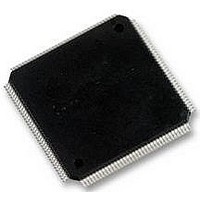
LFXP6C-5TN144C LATTICE SEMICONDUCTOR, LFXP6C-5TN144C Datasheet - Page 23

LFXP6C-5TN144C
Manufacturer Part Number
LFXP6C-5TN144C
Description
FPGA, 1.8V FLASH, INSTANT ON, SMD
Manufacturer
LATTICE SEMICONDUCTOR
Series
LatticeXPr
Datasheet
1.LFXP3C-3QN208C.pdf
(130 pages)
Specifications of LFXP6C-5TN144C
No. Of Logic Blocks
720
No. Of Macrocells
3000
Family Type
LatticeXP
No. Of Speed Grades
5
No. Of I/o's
100
Clock Management
PLL
Core Supply Voltage Range
1.71V To 3.465V
Lead Free Status / RoHS Status
Lead free / RoHS Compliant
Available stocks
Company
Part Number
Manufacturer
Quantity
Price
Company:
Part Number:
LFXP6C-5TN144C
Manufacturer:
LATTICE
Quantity:
2 291
Company:
Part Number:
LFXP6C-5TN144C
Manufacturer:
Lattice
Quantity:
60
Company:
Part Number:
LFXP6C-5TN144C
Manufacturer:
Lattice Semiconductor Corporation
Quantity:
10 000
Company:
Part Number:
LFXP6C-5TN144C-4I
Manufacturer:
LATTICE
Quantity:
2 291
Lattice Semiconductor
Figure 2-25. Tristate Register Block
Control Logic Block
The control logic block allows the selection and modification of control signals for use in the PIO block. A clock is
selected from one of the clock signals provided from the general purpose routing and a DQS signal provided from
the programmable DQS pin. The clock can optionally be inverted.
The clock enable and local reset signals are selected from the routing and optionally inverted. The global tristate
signal is passed through this block.
DDR Memory Support
Implementing high performance DDR memory interfaces requires dedicated DDR register structures in the input
(for read operations) and in the output (for write operations). As indicated in the PIO Logic section, the LatticeXP
devices provide this capability. In addition to these registers, the LatticeXP devices contain two elements to simplify
the design of input structures for read operations: the DQS delay block and polarity control logic.
DLL Calibrated DQS Delay Block
Source Synchronous interfaces generally require the input clock to be adjusted in order to correctly capture data at
the input register. For most interfaces a PLL is used for this adjustment, however in DDR memories the clock
(referred to as DQS) is not free running so this approach cannot be used. The DQS Delay block provides the
required clock alignment for DDR memory interfaces.
The DQS signal (selected PIOs only) feeds from the PAD through a DQS delay element to a dedicated DQS routing
resource. The DQS signal also feeds the polarity control logic which controls the polarity of the clock to the sync
registers in the input register blocks. Figures 2-26 and 2-27 show how the polarity control logic are routed to the
PIOs.
The temperature, voltage and process variations of the DQS delay block are compensated by a set of calibration
(6-bit bus) signals from two DLLs on opposite sides of the device. Each DLL compensates DQS Delays in its half of
the device as shown in Figure 2-27. The DLL loop is compensated for temperature, voltage and process variations
by the system clock and feedback loop.
Routing
From
ONEG1
OPOS1
TD
CLK1
*Latch is transparent when input is low.
/LATCH
D
D
D-Type
LATCH
LE*
Q
Q
2-20
0
1
Programmed
Control
OUTDDN
LatticeXP Family Data Sheet
0
1
To sysIO
TO
Buffer
Architecture


