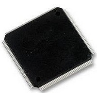
LFXP6C-5TN144C LATTICE SEMICONDUCTOR, LFXP6C-5TN144C Datasheet - Page 26

LFXP6C-5TN144C
Manufacturer Part Number
LFXP6C-5TN144C
Description
FPGA, 1.8V FLASH, INSTANT ON, SMD
Manufacturer
LATTICE SEMICONDUCTOR
Series
LatticeXPr
Datasheet
1.LFXP3C-3QN208C.pdf
(130 pages)
Specifications of LFXP6C-5TN144C
No. Of Logic Blocks
720
No. Of Macrocells
3000
Family Type
LatticeXP
No. Of Speed Grades
5
No. Of I/o's
100
Clock Management
PLL
Core Supply Voltage Range
1.71V To 3.465V
Lead Free Status / RoHS Status
Lead free / RoHS Compliant
Available stocks
Company
Part Number
Manufacturer
Quantity
Price
Company:
Part Number:
LFXP6C-5TN144C
Manufacturer:
LATTICE
Quantity:
2 291
Company:
Part Number:
LFXP6C-5TN144C
Manufacturer:
Lattice
Quantity:
60
Company:
Part Number:
LFXP6C-5TN144C
Manufacturer:
Lattice Semiconductor Corporation
Quantity:
10 000
Company:
Part Number:
LFXP6C-5TN144C-4I
Manufacturer:
LATTICE
Quantity:
2 291
Lattice Semiconductor
Figure 2-28. LatticeXP Banks
LatticeXP devices contain two types of sysIO buffer pairs.
1. Top and Bottom sysIO Buffer Pair (Single-Ended Outputs Only)
2. Left and Right sysIO Buffer Pair (Differential and Single-Ended Outputs)
The sysIO buffer pairs in the top and bottom banks of the device consist of two single-ended output drivers and
two sets of single-ended input buffers (both ratioed and referenced). The referenced input buffer can also be
configured as a differential input.
The two pads in the pair are described as “true” and “comp”, where the true pad is associated with the positive
side of the differential input buffer and the comp (complementary) pad is associated with the negative side of
the differential input buffer.
Only the I/Os on the top and bottom banks have PCI clamps. Note that the PCI clamp is enabled after V
V
The sysIO buffer pairs in the left and right banks of the device consist of two single-ended output drivers, two
sets of single-ended input buffers (both ratioed and referenced) and one differential output driver. The refer-
enced input buffer can also be configured as a differential input. In these banks the two pads in the pair are
described as “true” and “comp”, where the true pad is associated with the positive side of the differential I/O,
and the comp (complementary) pad is associated with the negative side of the differential I/O.
Select I/Os in the left and right banks have LVDS differential output drivers. Refer to the Logic Signal Connec-
tions tables for more information.
CCAUX
and V
CCIO
are at valid operating levels and the device has been configured.
V
V
V
V
V
GND
V
GND
Note: N and M are the maximum number of I/Os per bank.
REF1(7)
REF2(7)
CCIO7
CCIO6
REF2(6)
REF1(6)
M
M
1
1
1
1
Bank 0
Bank 5
N
N
2-23
1
1
Bank 1
Bank 4
M
M
N
1
1
N
LatticeXP Family Data Sheet
V
V
V
V
V
V
GND
GND
REF1(2)
REF2(2)
REF2(3)
REF1(3)
CCIO2
CCIO3
Architecture
CC,


