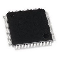
LCMXO256C-5TN100C LATTICE SEMICONDUCTOR, LCMXO256C-5TN100C Datasheet - Page 16

LCMXO256C-5TN100C
Manufacturer Part Number
LCMXO256C-5TN100C
Description
MACHXO PLD FLASH, SCRAM 1.8V, 256
Manufacturer
LATTICE SEMICONDUCTOR
Series
MachXOr
Datasheet
1.LCMXO1200C-5TN144C.pdf
(244 pages)
Specifications of LCMXO256C-5TN100C
Cpld Type
FLASH
No. Of Macrocells
128
No. Of I/o's
78
Propagation Delay
3.5ns
Global Clock Setup Time
1.3ns
Frequency
600MHz
Supply Voltage Range
1.71V To 3.465V
Operating
RoHS Compliant
Available stocks
Company
Part Number
Manufacturer
Quantity
Price
Company:
Part Number:
LCMXO256C-5TN100C
Manufacturer:
Lattice Semiconductor Corporation
Quantity:
10 000
- Current page: 16 of 244
- Download datasheet (9Mb)
Lattice Semiconductor
The ispLEVER design tool takes the output of the synthesis tool and places and routes the design. Generally, the
place and route tool is completely automatic, although an interactive routing editor is available to optimize the
design.
Clock/Control Distribution Network
The MachXO family of devices provides global signals that are available to all PFUs. These signals consist of four
primary clocks and four secondary clocks. Primary clock signals are generated from four 16:1 muxes as shown in
Figure 2-7 and Figure 2-8. The available clock sources for the MachXO256 and MachXO640 devices are four dual
function clock pins and 12 internal routing signals. The available clock sources for the MachXO1200 and
MachXO2280 devices are four dual function clock pins, up to nine internal routing signals and up to six PLL out-
puts.
Figure 2-7. Primary Clocks for MachXO256 and MachXO640 Devices
Routing
12
Clock
Pads
4
2-7
16:1
16:1
16:1
16:1
Primary Clock 0
Primary Clock 1
Primary Clock 2
Primary Clock 3
MachXO Family Data Sheet
Architecture
Related parts for LCMXO256C-5TN100C
Image
Part Number
Description
Manufacturer
Datasheet
Request
R
Part Number:
Description:
IC, CPLD, FLASH, 256 MACROCELL, TQFP-100
Manufacturer:
LATTICE SEMICONDUCTOR

Part Number:
Description:
IC, CPLD, FLASH, 256 MACROCELL, TQFP-100
Manufacturer:
LATTICE SEMICONDUCTOR
Part Number:
Description:
CPLD MachXO Family 128 Macro Cells 1.8V/2.5V/3.3V 100-Pin TQFP Tray
Manufacturer:
LATTICE SEMICONDUCTOR
Datasheet:
Part Number:
Description:
ISPLSI2032-80LT44Lattice Semiconductor [In-System Programmable High Density PLD]
Manufacturer:
Lattice Semiconductor Corp.
Datasheet:
Part Number:
Description:
IC PROGRAMMED LATTICE GAL 16V8
Manufacturer:
Lattice Semiconductor Corp.
Datasheet:
Part Number:
Description:
357-036-542-201 CARDEDGE 36POS DL .156 BLK LOPRO
Manufacturer:
Lattice Semiconductor Corp.
Datasheet:
Part Number:
Description:
357-036-542-201 CARDEDGE 36POS DL .156 BLK LOPRO
Manufacturer:
Lattice Semiconductor Corp.
Datasheet:
Part Number:
Description:
357-036-542-201 CARDEDGE 36POS DL .156 BLK LOPRO
Manufacturer:
Lattice Semiconductor Corp.
Datasheet:
Part Number:
Description:
357-036-542-201 CARDEDGE 36POS DL .156 BLK LOPRO
Manufacturer:
Lattice Semiconductor Corp.
Datasheet:
Part Number:
Description:
357-036-542-201 CARDEDGE 36POS DL .156 BLK LOPRO
Manufacturer:
Lattice Semiconductor Corp.
Datasheet:
Part Number:
Description:
357-036-542-201 CARDEDGE 36POS DL .156 BLK LOPRO
Manufacturer:
Lattice Semiconductor Corp.
Datasheet:
Part Number:
Description:
357-036-542-201 CARDEDGE 36POS DL .156 BLK LOPRO
Manufacturer:
Lattice Semiconductor Corp.
Datasheet:
Part Number:
Description:
357-036-542-201 CARDEDGE 36POS DL .156 BLK LOPRO
Manufacturer:
Lattice Semiconductor Corp.
Datasheet:
Part Number:
Description:
357-036-542-201 CARDEDGE 36POS DL .156 BLK LOPRO
Manufacturer:
Lattice Semiconductor Corp.
Datasheet:
Part Number:
Description:
357-036-542-201 CARDEDGE 36POS DL .156 BLK LOPRO
Manufacturer:
Lattice Semiconductor Corp.
Datasheet:


