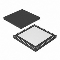
PIC24FJ256GA106-I/MR Microchip Technology, PIC24FJ256GA106-I/MR Datasheet - Page 18

PIC24FJ256GA106-I/MR
Manufacturer Part Number
PIC24FJ256GA106-I/MR
Description
IC, 16BIT MCU, PIC24F, 32MHZ, QFN-64
Manufacturer
Microchip Technology
Series
PIC® 24Fr
Datasheets
1.PIC24FJ128GA008-IPT.pdf
(12 pages)
2.PIC24FJ128GA106-IPT.pdf
(14 pages)
3.PIC24FJ128GA106-IPT.pdf
(330 pages)
4.PIC24FJ128GA106-IPT.pdf
(52 pages)
5.PIC24FJ256GA106-IPT.pdf
(59 pages)
6.PIC24FJ128GB110-IPF.pdf
(292 pages)
Specifications of PIC24FJ256GA106-I/MR
Controller Family/series
PIC24
No. Of I/o's
53
Ram Memory Size
16KB
Cpu Speed
32MHz
No. Of Timers
5
Core Size
16 Bit
Program Memory Size
256KB
Peripherals
ADC, Comparator, PWM, RTC, Timer
Core Processor
PIC
Speed
32MHz
Connectivity
I²C, PMP, SPI, UART/USART
Number Of I /o
53
Program Memory Type
FLASH
Ram Size
16K x 8
Voltage - Supply (vcc/vdd)
2 V ~ 3.6 V
Data Converters
A/D 16x10b
Oscillator Type
Internal
Operating Temperature
-40°C ~ 85°C
Package / Case
64-VFQFN, Exposed Pad
Processor Series
PIC24FJ
Core
PIC
Data Bus Width
16 bit
Data Ram Size
16 KB
Interface Type
I2C, SPI, UART
Maximum Clock Frequency
32 MHz
Number Of Programmable I/os
52
Number Of Timers
5
Maximum Operating Temperature
+ 85 C
Mounting Style
SMD/SMT
3rd Party Development Tools
52713-733, 52714-737, 53276-922, EWDSPIC
Development Tools By Supplier
PG164130, DV164035, DV244005, DV164005, PG164120, DM240001, DM240011
Minimum Operating Temperature
- 40 C
On-chip Adc
10 bit, 16 Channel
Lead Free Status / RoHS Status
Lead free / RoHS Compliant
For Use With
876-1004 - PIC24 BREAKOUT BOARD
Eeprom Size
-
Lead Free Status / Rohs Status
Details
PIC24FJXXXDA1/DA2/GB2/GA3
3.4
3.4.1
Flash memory write and erase operations are
controlled by the NVMCON register. Programming is
performed by setting NVMCON to select the type of
erase operation (see
Table
WR control bit (NVMCON<15>).
In ICSP mode, all programming operations are
self-timed. There is an internal delay between the user
setting the WR control bit and the automatic clearing of
the WR control bit when the programming operation is
complete. Refer to
tics and Timing Requirements”
the delays associated with various programming
operations.
TABLE 3-2:
TABLE 3-3:
3.4.2
The WR bit (NVMCON<15>) is used to start an erase or
write cycle. Setting the WR bit initiates the programming
cycle.
All erase and write cycles are self-timed. The WR bit
should be polled to determine if the erase or write cycle
has been completed. Starting a programming cycle is
performed as follows:
DS39970B-page 18
404Fh
4042h
4003h
4001h
NVMCON
NVMCON
Value
Value
BSET
3-3) and initiating the programming by setting the
Flash Memory Programming in
ICSP Mode
PROGRAMMING OPERATIONS
STARTING AND STOPPING A
PROGRAMMING CYCLE
Write a single code memory word,
Configuration Word or Executive Memory
Word.
Program 1 row (64 instruction words) of
code memory or executive memory.
Erase a page of code memory or
Erase all code memory, executive
memory and Configuration registers
(does not erase Device ID registers).
executive memory.
NVMCON, #WR
NVMCON ERASE
OPERATIONS
NVMCON WRITE
OPERATIONS
Section 7.0 “AC/DC Characteris-
Table
Erase Operation
Write Operation
3-2) or write operation (see
for information about
3.5
The procedure for erasing program memory (all of the
code memory, data memory, executive memory and
code-protect bits) consists of setting NVMCON to
404Fh and executing the programming cycle.
A Chip Erase can erase all of the user memory or all of
both the user and configuration memory. A Table Write
instruction should be executed prior to performing the
Chip Erase to select which sections are erased.
The Table Write instruction is executed:
• If the TBLPAG register points to user space (is
• If the TBLPAG register points to configuration
Figure 3-5
performing a Chip Erase. This process includes the
ICSP command code, which must be transmitted (for
each instruction), LSb first, using the PGECx and
PGEDx pins (see
FIGURE 3-5:
less than 0x80), the Chip Erase will erase only
user memory and Flash Configuration Words.
space (is greater than or equal to 0x80), the Chip
Erase is not allowed. The configuration space can
be erased one page at a time.
Note:
Note:
Erasing Program Memory
displays the ICSP programming process for
The Chip Erase is not allowed when the
TBLPAG points to the configuration space
to avoid the Diagnostic and Calibration
Words from getting erased.
Program memory must be erased before
writing any data to program memory.
Set the WR bit to Initiate Erase
No
Write 404Fh to NVMCON SFR
Figure
cleared (‘
CHIP ERASE FLOW
Is WR bit
Yes
2010 Microchip Technology Inc.
3-2).
Start
End
0
’)?


