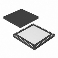
PIC24FJ256GA106-I/MR Microchip Technology, PIC24FJ256GA106-I/MR Datasheet - Page 23

PIC24FJ256GA106-I/MR
Manufacturer Part Number
PIC24FJ256GA106-I/MR
Description
IC, 16BIT MCU, PIC24F, 32MHZ, QFN-64
Manufacturer
Microchip Technology
Series
PIC® 24Fr
Datasheets
1.PIC24FJ128GA008-IPT.pdf
(12 pages)
2.PIC24FJ128GA106-IPT.pdf
(14 pages)
3.PIC24FJ128GA106-IPT.pdf
(330 pages)
4.PIC24FJ128GA106-IPT.pdf
(52 pages)
5.PIC24FJ256GA106-IPT.pdf
(59 pages)
6.PIC24FJ128GB110-IPF.pdf
(292 pages)
Specifications of PIC24FJ256GA106-I/MR
Controller Family/series
PIC24
No. Of I/o's
53
Ram Memory Size
16KB
Cpu Speed
32MHz
No. Of Timers
5
Core Size
16 Bit
Program Memory Size
256KB
Peripherals
ADC, Comparator, PWM, RTC, Timer
Core Processor
PIC
Speed
32MHz
Connectivity
I²C, PMP, SPI, UART/USART
Number Of I /o
53
Program Memory Type
FLASH
Ram Size
16K x 8
Voltage - Supply (vcc/vdd)
2 V ~ 3.6 V
Data Converters
A/D 16x10b
Oscillator Type
Internal
Operating Temperature
-40°C ~ 85°C
Package / Case
64-VFQFN, Exposed Pad
Processor Series
PIC24FJ
Core
PIC
Data Bus Width
16 bit
Data Ram Size
16 KB
Interface Type
I2C, SPI, UART
Maximum Clock Frequency
32 MHz
Number Of Programmable I/os
52
Number Of Timers
5
Maximum Operating Temperature
+ 85 C
Mounting Style
SMD/SMT
3rd Party Development Tools
52713-733, 52714-737, 53276-922, EWDSPIC
Development Tools By Supplier
PG164130, DV164035, DV244005, DV164005, PG164120, DM240001, DM240011
Minimum Operating Temperature
- 40 C
On-chip Adc
10 bit, 16 Channel
Lead Free Status / RoHS Status
Lead free / RoHS Compliant
For Use With
876-1004 - PIC24 BREAKOUT BOARD
Eeprom Size
-
Lead Free Status / Rohs Status
Details
3.7
Device configuration for PIC24FJXXXDA1/DA2/GB2/
GA3 devices is stored in Flash Configuration Words at
the end of the user space program memory and in
multiple register Configuration Words, located in the test
space. These registers reflect values read at any Reset
from program memory locations. The values for the Con-
figuration Words for the default device configurations are
listed in
The values can be changed only by programming the
content of the corresponding Flash Configuration Word
and resetting the device. The Reset forces an auto-
matic reload of the Flash stored configuration values by
sequencing through the dedicated Flash Configuration
Words and transferring the data into the Configuration
registers.
For the PIC24FJXXXDA1/DA2/GB2/GA3 families, cer-
tain Configuration bits have default states that must
always be maintained to ensure device functionality,
regardless of the settings of other Configuration bits.
To change the values of the Flash Configuration Word
once it has been programmed, the device must be Chip
Erased, as described in
Memory”
not possible to program a ‘0’ to ‘1’; they may be
programmed from a ‘1’ to ‘0’ to enable code protection.
TABLE 3-6:
2010 Microchip Technology Inc.
Last Word
Last Word – 2
Last Word – 4
Last Word – 6
Address
Table
Writing Configuration Words
and reprogrammed to the desired value. It is
3-6.
DEFAULT CONFIGURATION
REGISTER VALUES
Section 3.5 “Erasing Program
Name
CW1
CW2
CW3
CW4
PIC24FJXXXDA1/DA2/GB2/GA3
Default Value
FFFFh
FFFFh
FFFFh
7FFFh
Table 3-7
programming the Configuration Word locations, includ-
ing the serial pattern with the ICSP command code,
which must be transmitted, LSb first, using the PGECx
and PGEDx pins (see
In Step 1, the Reset vector is exited. In Step 2, the lower
16 bits of the source address are stored in W7. In
Step 3, the NVMCON register is initialized for program-
ming of code memory. In Step 4, the upper byte of the
24-bit starting source address for writing is loaded into
the TBLPAG register.
The TBLPAG register must be loaded with 00h for
64 Kbytes, and 01h for 128 and 256 Kbytes devices.
To verify the data by reading the Configuration Words
after performing the write in order, the code protection
bits initially should be programmed to a ‘1’ to ensure
that the verification can be performed properly. After
verification is finished, the code protection bit can be
programmed to a ‘0’ by using a word write to the
appropriate Configuration Word.
provides the ICSP programming details for
Figure
3-2).
DS39970B-page 23


