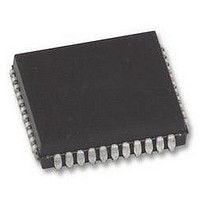
AT80C51RD2-SLSUM Atmel, AT80C51RD2-SLSUM Datasheet - Page 14

AT80C51RD2-SLSUM
Manufacturer Part Number
AT80C51RD2-SLSUM
Description
MCU, 8BIT, 8051, 5V, SPI, 20MHZ, 44PLCC
Manufacturer
Atmel
Specifications of AT80C51RD2-SLSUM
Controller Family/series
(8051) 8052
No. Of I/o's
32
Ram Memory Size
1280Byte
Cpu Speed
40MHz
No. Of Timers
3
No. Of Pwm Channels
5
Core Size
8bit
Oscillator Type
External Only
Processor Series
AT80x
Core
8051
Data Bus Width
8 bit
Program Memory Type
ROMLess
Data Ram Size
1280 B
Interface Type
UART, SPI
Maximum Clock Frequency
60 MHz
Number Of Programmable I/os
32
Number Of Timers
3
Operating Supply Voltage
2.7 V to 5.5 V
Maximum Operating Temperature
+ 85 C
Mounting Style
SMD/SMT
Package / Case
PLCC
3rd Party Development Tools
PK51, CA51, A51, ULINK2
Minimum Operating Temperature
- 40 C
Cpu Family
AT80
Device Core
8051
Device Core Size
8b
Frequency (max)
40MHz
Program Memory Size
Not Required
Total Internal Ram Size
1.25KB
# I/os (max)
32
Number Of Timers - General Purpose
3
Operating Supply Voltage (typ)
3.3/5V
Operating Supply Voltage (max)
5.5V
Operating Supply Voltage (min)
2.7V
Instruction Set Architecture
CISC
Operating Temp Range
-40C to 85C
Operating Temperature Classification
Industrial
Mounting
Surface Mount
Pin Count
44
Package Type
PLCC
Lead Free Status / RoHS Status
Lead free / RoHS Compliant
Lead Free Status / RoHS Status
Lead free / RoHS Compliant
Available stocks
Company
Part Number
Manufacturer
Quantity
Price
Company:
Part Number:
AT80C51RD2-SLSUM
Manufacturer:
Atmel
Quantity:
1 445
8. Expanded RAM (XRAM)
Figure 8-1.
14
AT80C51RD2
0FFh or 3FFh
Internal and External Data Memory Address
00
The AT80C51RD2 devices provide additional Bytes of Random Access Memory (RAM) space
for increased data parameter handling and high level language usage.
The devices have expanded RAM in external data space; maximum size and location are
described in Table 8-1.
Table 8-1.
The AT80C51RD2 has internal data memory that is mapped into four separate segments.
The four segments are:
The lower 128 bytes can be accessed by either direct or indirect addressing. The Upper 128
bytes can be accessed by indirect addressing only. The Upper 128 bytes occupy the same
address space as the SFR. That means they have the same address, but are physically sepa-
rate from SFR space.
When an instruction accesses an internal location above address 7Fh, the CPU knows whether
the access is to the upper 128 bytes of data RAM or to SFR space by the addressing mode used
in the instruction.
T83C51RB2/RC2
T80C51RD2
1. The Lower 128 bytes of RAM (addresses 00h to 7Fh) are directly and indirectly
2. The Upper 128 bytes of RAM (addresses 80h to FFh) are indirectly addressable only.
3. The Special Function Registers (SFRs) (addresses 80h to FFh) are directly address-
4. The expanded RAM bytes are indirectly accessed by MOVX instructions, and with the
• Instructions that use direct addressing access SFR space. For example: MOV 0A0H, # data,
XRAM
accesses the SFR at location 0A0h (which is P2).
addressable.
able only.
EXTRAM bit cleared in the AUXR register (see Table 8-1).
0FFh
Expanded RAM
80h
7Fh
00
indirect accesses
Direct or Indirect
128 Bytes
128 Bytes
Accesses
Internal
Internal
Upper
Lower
RAM
RAM
XRAM size
1024
0FFh
80h
Direct Accesses
Function
Register
Special
00FFh up to 03FFh
Start
00h
0FFFFh
0000
Address
External
Memory
Data
3FFh
4113D–8051–01/09
End


