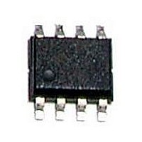
MB95F214KPF-G-SNE2 Fujitsu, MB95F214KPF-G-SNE2 Datasheet - Page 15

MB95F214KPF-G-SNE2
Manufacturer Part Number
MB95F214KPF-G-SNE2
Description
IC, MCU, 8BIT, 16K FLASH, 8FX, 8SOP
Manufacturer
Fujitsu
Datasheet
1.MB95F204KPF-G-SNE2.pdf
(72 pages)
Specifications of MB95F214KPF-G-SNE2
No. Of I/o's
5
Ram Memory Size
496Byte
Cpu Speed
16.25MHz
No. Of Timers
1
No. Of Pwm Channels
1
Core Size
8bit
Program Memory Size
16KB
Oscillator Type
Internal, External
Controller Family/series
MB95210H
Available stocks
Company
Part Number
Manufacturer
Quantity
Price
Company:
Part Number:
MB95F214KPF-G-SNE2
Manufacturer:
Fujitsu
Quantity:
100
■ NOTES ON DEVICE HANDLING
• Preventing latch-ups
• Stabilizing supply voltage
• Notes on using the external clock
■ PIN CONNECTION
• Treatment of unused pins
• Power supply pins
• DBG pin
• RSTX pin
DS07-12623-5E
When using the device, ensure that the voltage applied does not exceed the maximum voltage rating.
In a CMOS IC, if a voltage higher than V
neither a medium-withstand voltage pin nor a high-withstand voltage pin, or if a voltage out of the rating range
of power supply voltage mentioned in “1. Absolute Maximum Ratings” of ■ ELECTRICAL CHARACTERISTICS”
is applied to the V
When a latch-up occurs, power supply current increases significantly, which may cause a component to be
thermally destroyed.
Supply voltage must be stabilized.
A malfunction may occur when power supply voltage fluctuates rapidly even though the fluctuation is within the
guaranteed operating range of the V
As a rule of voltage stabilization, suppress voltage fluctuation so that the fluctuation in V
the commercial frequency (50 Hz/60 Hz) does not exceed 10% of the standard V
fluctuation rate does not exceed 0.1 V/ms at a momentary fluctuation such as switching the power supply.
When an external clock is used, oscillation stabilization wait time is required for power-on reset, wake-up from
subclock mode or stop mode.
If an unused input pin is left unconnected, a component may be permanently damaged due to malfunctions or
latch-ups. Always pull up or pull down an unused input pin through a resistor of at least 2 kΩ. Set an unused
input/output pin to the output state and leave it unconnected, or set it to the input state and treat it the same as
an unused input pin. If there is an unused output pin, leave it unconnected.
To reduce unnecessary electro-magnetic emission, prevent malfunctions of strobe signals due to an increase
in the ground level, and conform to the total output current standard, always connect the V
to the power supply and ground outside the device. In addition, connect the current supply source to the V
and the V
It is also advisable to connect a ceramic bypass capacitor of approximately 0.1 µF between the V
V
Connect the DBG pin directly to an external pull-up resistor.
To prevent the device from unintentionally entering the debug mode due to noise, minimize the distance between
the DBG pin and the V
The DBG pin should not stay at “L” level after power-on until the reset output is released.
Connect the RSTX pin directly to an external pull-up resistor.
To prevent the device from unintentionally entering the reset mode due to noise, minimize the distance between
the RSTX pin and the V
The RSTX/PF2 pin functions as the reset input/output pin after power-on. In addition, the reset output can be
enabled by the RSTOE bit of the SYSC register, and the reset input function or the general purpose I/O function
can be selected by the RSTEN bit of the SYSC register.
SS
pin at a location close to this device.
SS
pin with low impedance.
CC
pin or the V
CC
CC
or V
or V
SS
SS
pin when designing the layout of the printed circuit board.
SS
pin when designing the layout of the printed circuit board.
pin, a latch-up may occur.
CC
power supply voltage.
CC
or a voltage lower than V
MB95200H/210H Series
SS
is applied to an input/output pin that is
CC
value, and the transient
CC
CC
ripple (p-p value) at
pin and the V
CC
pin and the
CC
SS
pin
pin
15


