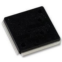
LFXP2-17E-5QN208C8W LATTICE SEMICONDUCTOR, LFXP2-17E-5QN208C8W Datasheet - Page 47

LFXP2-17E-5QN208C8W
Manufacturer Part Number
LFXP2-17E-5QN208C8W
Description
FPGA, 17K LUTS, 146 IO, DSP, 208PQFP
Manufacturer
LATTICE SEMICONDUCTOR
Series
LatticeXP2r
Datasheet
1.LFXP2-5E-5TN144C.pdf
(93 pages)
Specifications of LFXP2-17E-5QN208C8W
No. Of Macrocells
8500
Family Type
LatticeXP2
No. Of Speed Grades
5
No. Of I/o's
146
Clock Management
PLL
Core Supply Voltage Range
1.14V To 1.26V
I/o Supply
RoHS Compliant
- Current page: 47 of 93
- Download datasheet (2Mb)
Lattice Semiconductor
Supply Current (Standby)
I
I
I
I
I
1. For further information on supply current, please see TN1139, Power Estimation and Management for LatticeXP2 Devices.
2. Assumes all outputs are tristated, all inputs are configured as LVCMOS and held at the V
3. Frequency 0MHz.
4. Pattern represents a “blank” configuration data file.
5. T
6. In fpBGA and ftBGA packages the PLLs are connected to and powered from the auxiliary power supply. For these packages,
CC
CCAUX
CCPLL
CCIO
CCJ
the actual auxiliary supply current is the sum of I
powered independent of the auxiliary power supply.
J
= 25
Symbol
o
C, power supplies at nominal voltage.
Core Power Supply Current
Auxiliary Power Supply Current
PLL Power Supply Current (per PLL)
Bank Power Supply Current (per bank)
V
CCJ
Power Supply Current
Over Recommended Operating Conditions
1, 2, 3, 4
Parameter
CCAUX
6
and I
3-3
CCPLL.
For csBGA, PQFP and TQFP packages the PLLs are
XP2-5
XP2-8
XP2-17
XP2-30
XP2-40
XP2-5
XP2-8
XP2-17
XP2-30
XP2-40
Device
DC and Switching Characteristics
LatticeXP2 Family Data Sheet
CCIO
or GND.
Typical
0.25
0.1
14
18
24
35
45
15
15
15
16
16
2
5
Units
mA
mA
mA
mA
mA
mA
mA
mA
mA
mA
mA
mA
mA
Related parts for LFXP2-17E-5QN208C8W
Image
Part Number
Description
Manufacturer
Datasheet
Request
R

Part Number:
Description:
IC, LATTICEXP2 FPGA, 435MHZ, FPBGA-484
Manufacturer:
LATTICE SEMICONDUCTOR
Datasheet:

Part Number:
Description:
Development Tools & Eval/Demo Boards
Manufacturer:
LATTICE SEMICONDUCTOR
Datasheet:
Part Number:
Description:
FPGA LatticeXP2 Family 17000 Cells Flash Technology 1.2V 484-Pin FBGA
Manufacturer:
LATTICE SEMICONDUCTOR
Datasheet:
Part Number:
Description:
FPGA LatticeXP2 Family 17000 Cells Flash Technology 1.2V 484-Pin FBGA
Manufacturer:
LATTICE SEMICONDUCTOR
Datasheet:
Part Number:
Description:
FPGA LatticeXP2 Family 17000 Cells Flash Technology 1.2V 484-Pin FBGA
Manufacturer:
LATTICE SEMICONDUCTOR
Datasheet:
Part Number:
Description:
Latticexp2 Fpga Data Sheets
Manufacturer:
Lattice Semiconductor Corp.
Datasheet:

Part Number:
Description:
FPGA - Field Programmable Gate Array 5K LUTs 146I/O Inst- on DSP 1.2V -5 Spd
Manufacturer:
Lattice
Datasheet:

Part Number:
Description:
FPGA - Field Programmable Gate Array 5K LUTs 172I/O Inst- on DSP 1.2V -5 Spd
Manufacturer:
Lattice
Datasheet:

Part Number:
Description:
FPGA - Field Programmable Gate Array 5K LUTs 100I/O Inst- on DSP 1.2V -5 Spd
Manufacturer:
Lattice
Datasheet:
Part Number:
Description:
ISPLSI2032-80LT44Lattice Semiconductor [In-System Programmable High Density PLD]
Manufacturer:
Lattice Semiconductor Corp.
Datasheet:
Part Number:
Description:
IC PROGRAMMED LATTICE GAL 16V8
Manufacturer:
Lattice Semiconductor Corp.
Datasheet:
Part Number:
Description:
357-036-542-201 CARDEDGE 36POS DL .156 BLK LOPRO
Manufacturer:
Lattice Semiconductor Corp.
Datasheet:
Part Number:
Description:
357-036-542-201 CARDEDGE 36POS DL .156 BLK LOPRO
Manufacturer:
Lattice Semiconductor Corp.
Datasheet:
Part Number:
Description:
357-036-542-201 CARDEDGE 36POS DL .156 BLK LOPRO
Manufacturer:
Lattice Semiconductor Corp.
Datasheet:
Part Number:
Description:
357-036-542-201 CARDEDGE 36POS DL .156 BLK LOPRO
Manufacturer:
Lattice Semiconductor Corp.
Datasheet:


