ADXRS401ABG-REEL Analog Devices Inc, ADXRS401ABG-REEL Datasheet - Page 8
ADXRS401ABG-REEL
Manufacturer Part Number
ADXRS401ABG-REEL
Description
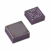
IC GYROSCOPE SGL COND 32CSPBGA
Manufacturer
Analog Devices Inc
Datasheet
1.ADXRS401ABG.pdf
(12 pages)
Specifications of ADXRS401ABG-REEL
Range °/s
±75°/s
Sensitivity
15mV/°/s
Typical Bandwidth
40Hz
Voltage - Supply
4.75 V ~ 5.25 V
Current - Supply
6mA
Output Type
Ratiometric
Operating Temperature
-40°C ~ 85°C
Package / Case
32-CSPBGA
For Use With
ADXRS401EB - EVAL BOARD FOR ADXRS401ABG
Lead Free Status / RoHS Status
Contains lead / RoHS non-compliant


ADXRS401
THEORY OF OPERATION
The ADXRS401 operates on the principle of a resonator gyro.
Two polysilicon sensing structures each contain a dither frame,
which is electrostatically driven to resonance. This produces the
necessary velocity element to produce a Coriolis force during
angular rate. At two of the outer extremes of each frame,
orthogonal to the dither motion, are movable fingers that are
placed between fixed pickoff fingers to form a capacitive pickoff
structure that senses Coriolis motion.
The resulting signal is fed to a series of gain and demodulation
stages that produce the electrical rate signal output. The dual-
sensor design rejects external g-forces and vibration.
Fabricating the sensor with the signal conditioning electronics
preserves signal integrity in noisy environments.
The electrostatic resonator requires 14 V to 16 V for operation.
Since only 5 V is typically available in most applications, a
charge pump is included on-chip. If an external 14 V to 16 V
supply is available, the two capacitors on CP1 to CP4 can be
omitted and this supply can be connected to CP5 (Pin 7D) with
a 1 µF decoupling capacitor.
After the demodulation stage there is a single-pole low-pass
filter consisting of an internal 9 kΩ resistor (R
external user-supplied capacitor (CMID). A CMID capacitor of
100 nF sets a 400 Hz low-pass pole ± 35% and is used to limit
high frequency artifacts before final amplification. A bandwidth
limit capacitor, C
Bandwidth section).
OUT
, sets the pass bandwidth (see Setting
Note that inner rows/columns of pins have been omitted for clarity but should be connected in the application.
5V
22nF
CP1
CP2
AVCC
SEN1
PGND
Figure 14. Example Application Circuit (Top View)
) and an
RATEOUT
5A
6A
4A
2A
3A
C
OUT
7B
1B
CP4
SUMJ
Rev. 0 | Page 8 of 12
= 22nF
22nF
7C
1C
CP3
CP5
100nF
1D
7D
CMID
100nF
SUPPLY AND COMMON CONSIDERATIONS
Only power supplies used for supplying analog circuits are
recommended for powering the ADXRS401. High frequency
noise and transients associated with digital circuit supplies may
have adverse affects on device operation. 1 µF shows the
recommended connections for the ADXRS401 where both
AVCC and PDD have a separate decoupling capacitor. These
should be placed as close to their respective pins as possible
before routing to the system analog supply. This will minimize
the noise injected by the charge pump that uses the PDD supply.
It is also recommended to place the charge pump capacitors
connected to the CP1 to CP4 pins as close to the part as
possible. These capacitors are used to produce the on-chip high
voltage supply switched at the dither frequency at
approximately 14 kHz. Care should be taken to ensure that
there is no more than 50 pF of stray capacitance between CP1
to CP4 and ground. Surface-mount chip capacitors are suitable
as long as they are rated for over 15 V.
1µF
1E
7E
2.5V
100nF
PDD
AGND
PGND
1F
7F
5G
6G
4G
3G
2G
CP4
ST1
ST2
TEMP
Related parts for ADXRS401ABG-REEL
Image
Part Number
Description
Manufacturer
Datasheet
Request
R

Part Number:
Description:
±1.7g Dual-Axis IMEMS Accelerometer Evaluation Board
Manufacturer:
Analog Devices Inc
Datasheet:

Part Number:
Description:
Inertial Sensor Evaluation System
Manufacturer:
Analog Devices Inc
Datasheet:
Part Number:
Description:
Manufacturer:
Analog Devices Inc
Datasheet:
Part Number:
Description:
Manufacturer:
Analog Devices Inc
Datasheet:
Part Number:
Description:
Manufacturer:
Analog Devices Inc
Datasheet:
Part Number:
Description:
Manufacturer:
Analog Devices Inc
Datasheet:
Part Number:
Description:
Manufacturer:
Analog Devices Inc
Datasheet:
Part Number:
Description:
Manufacturer:
Analog Devices Inc
Datasheet:
Part Number:
Description:
Manufacturer:
Analog Devices Inc
Datasheet:
Part Number:
Description:
Manufacturer:
Analog Devices Inc
Datasheet:
Part Number:
Description:
Manufacturer:
Analog Devices Inc
Datasheet:
Part Number:
Description:
Manufacturer:
Analog Devices Inc
Datasheet:
Part Number:
Description:
Manufacturer:
Analog Devices Inc
Datasheet: