ADXRS401ABG-REEL Analog Devices Inc, ADXRS401ABG-REEL Datasheet - Page 9
ADXRS401ABG-REEL
Manufacturer Part Number
ADXRS401ABG-REEL
Description
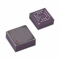
IC GYROSCOPE SGL COND 32CSPBGA
Manufacturer
Analog Devices Inc
Datasheet
1.ADXRS401ABG.pdf
(12 pages)
Specifications of ADXRS401ABG-REEL
Range °/s
±75°/s
Sensitivity
15mV/°/s
Typical Bandwidth
40Hz
Voltage - Supply
4.75 V ~ 5.25 V
Current - Supply
6mA
Output Type
Ratiometric
Operating Temperature
-40°C ~ 85°C
Package / Case
32-CSPBGA
For Use With
ADXRS401EB - EVAL BOARD FOR ADXRS401ABG
Lead Free Status / RoHS Status
Contains lead / RoHS non-compliant


SETTING BANDWIDTH
External capacitors CMID and C
with on-chip resistors to create two low-pass filters to limit the
bandwidth of the ADXRS401’s rate response. The –3 dB
frequency set by R
This frequency can be well controlled since R
trimmed during manufacturing to be 180 kΩ ±1%. Any external
resistor applied between the RATEOUT (1B, 2A) and SUMJ
(1C, 2C) pins will result in:
The −3 dB frequency is set by RSEN (the parallel combination
of R
controlled, because R
rate sensitivity during manufacturing and have a ±35%
tolerance. Its primary purpose is to limit the high frequency
demodulation artifacts from saturating the final amplifier stage.
Thus, this pole of nominally 400 Hz @ 0.1 µF need not be
precise. Lower frequency is preferable, but its variability usually
requires it to be about 10 times greater (in order to preserve
phase integrity) than the well-controlled output pole. In general,
both −3 dB filter frequencies should be set as low as possible to
reduce the amplitude of these high frequency artifacts, as well as
to reduce the overall system noise.
SEN1
R
f
OUT
OUT
and R
=
=
(
1/
180
SEN2
(
2
) at about 4.5 kΩ nominal. CMID is less well
kΩ
×
OUT
π
×
×
SEN1
and C
R
R
ST2
ST1
EXT
ADXRS401
OUT
and R
5G
4G
) (
OUT
/
×
180
C
SEN2
is:
OUT
OUT
kΩ
SELF
TEST
have been used to trim the
AVCC
CP2
)
are used in combination
+
4A
R
22nF
EXT
3A
+
SENSOR
5A
RATE
)
100nF
OUT
5V
CP1
Figure 15. Block Diagram with External Components
PDD
has been
–
CHARGE PUMP/REG.
2G
7E
PGND
100nF
CORIOLIS SIGNAL CHANNEL
RESONATOR LOOP
6G
Rev. 0 | Page 9 of 12
7F
1F
DEMOD
AGND
π
6A
100nF
CP4
INCREASING MEASUREMENT RANGE
To increase the full-scale measurement range of the ADXRS401,
place an external resistor between the RATEOUT (1B, 2A) and
SUMJ (1C, 2C) pins. This parallels the internal R
is factory-trimmed to 180 kΩ.
For example, a 330 kΩ external resistor gives approximately
10mV/°/sec sensitivity and a commensurate ∼50% increase in
the full-scale range. This is effective for up to a 4× increase in
the full-scale range. (The minimum value of the parallel resistor
allowed is 45 kΩ.) Beyond this amount of external sensitivity
reduction, the internal circuitry headroom requirements
prevent further increase in the linear full-scale output range.
The drawbacks of modifying the full-scale range are the
additional output null drift (as much as 2°/sec over
temperature) and the readjustment of the initial null bias. See
Null Adjust section and Application Note AN-625 for details.
TEMPERATURE OUTPUT AND CALIBRATION
It is common practice to temperature-calibrate gyros to
improve their overall accuracy. The ADXRS401 has a
temperature-proportional voltage output that provides input to
such a calibration method. The voltage at TEMP (3F, 3G) is
nominally 2.5 V at 27°C and has a PTAT (proportional to
absolute temperature) characteristic of 8.4 mV/°C. Note that the
TEMP output circuitry is limited to 50 µA source current.
Limiting the bandwidth of the device reduces the flat-band
noise during the calibration process, improving the
measurement accuracy at each calibration point.
≈
7B
12V
9kΩ
R
CMID
22nF
SEN
CP3
±
35%
1
2.5V REF
7C
1D
CP5
≈
9kΩ
S
7D
SEN
PTAT
±
2
35%
1µF
1C
SUMJ
180kΩ 1%
R
OUT
C
OUT
1B
2A
1E
3G
RATE-
OUT
2.5V
TEMP
ADXRS401
OUT
resistor that
Related parts for ADXRS401ABG-REEL
Image
Part Number
Description
Manufacturer
Datasheet
Request
R

Part Number:
Description:
±1.7g Dual-Axis IMEMS Accelerometer Evaluation Board
Manufacturer:
Analog Devices Inc
Datasheet:

Part Number:
Description:
Inertial Sensor Evaluation System
Manufacturer:
Analog Devices Inc
Datasheet:
Part Number:
Description:
Manufacturer:
Analog Devices Inc
Datasheet:
Part Number:
Description:
Manufacturer:
Analog Devices Inc
Datasheet:
Part Number:
Description:
Manufacturer:
Analog Devices Inc
Datasheet:
Part Number:
Description:
Manufacturer:
Analog Devices Inc
Datasheet:
Part Number:
Description:
Manufacturer:
Analog Devices Inc
Datasheet:
Part Number:
Description:
Manufacturer:
Analog Devices Inc
Datasheet:
Part Number:
Description:
Manufacturer:
Analog Devices Inc
Datasheet:
Part Number:
Description:
Manufacturer:
Analog Devices Inc
Datasheet:
Part Number:
Description:
Manufacturer:
Analog Devices Inc
Datasheet:
Part Number:
Description:
Manufacturer:
Analog Devices Inc
Datasheet:
Part Number:
Description:
Manufacturer:
Analog Devices Inc
Datasheet: