LY530AL STMicroelectronics, LY530AL Datasheet
LY530AL
Specifications of LY530AL
Available stocks


Related parts for LY530AL


LY530AL Summary of contents
Page 1
... LY530ALTR September 2008 This is preliminary information on a new product now in development or undergoing evaluation. Details are subject to change without notice. The output of LY530AL has a full scale of ±300 °/s and is capable of measuring rates with bandwidth Hz. The LY530AL is available in a plastic land grid array (LGA) package and can operate within a temperature range from -40 ° ...
Page 2
... Register mapping . . . . . . . . . . . . . . . . . . . . . . . . . . . . . . . . . . . . . . . . . . 23 6 Register description . . . . . . . . . . . . . . . . . . . . . . . . . . . . . . . . . . . . . . . . 24 6.1 WHO_AM_I (0Fh 6.2 CTRL_REG (20h 6.3 FILTER_CFG_REG (22h 2/30 SPI - serial peripheral interface . . . . . . . . . . . . . . . . . . . . . . . . . . . . . . . 11 I2C - Inter IC control interface . . . . . . . . . . . . . . . . . . . . . . . . . . . . . . . . 12 Sensitivity . . . . . . . . . . . . . . . . . . . . . . . . . . . . . . . . . . . . . . . . . . . . . . . . 14 Zero-rate level . . . . . . . . . . . . . . . . . . . . . . . . . . . . . . . . . . . . . . . . . . . . 14 Self-test . . . . . . . . . . . . . . . . . . . . . . . . . . . . . . . . . . . . . . . . . . . . . . . . . 14 I2C operation . . . . . . . . . . . . . . . . . . . . . . . . . . . . . . . . . . . . . . . . . . . . . 18 SPI read . . . . . . . . . . . . . . . . . . . . . . . . . . . . . . . . . . . . . . . . . . . . . . . . . 21 SPI write . . . . . . . . . . . . . . . . . . . . . . . . . . . . . . . . . . . . . . . . . . . . . . . . 21 SPI read in 3-wires mode . . . . . . . . . . . . . . . . . . . . . . . . . . . . . . . . . . . 22 LY530AL ...
Page 3
... LY530AL 6.4 OUTPUT_SEL_REG (23h 6.5 STATUS_REG(27h 6.6 OUT_CONV_H(28h 6.7 OUT_CONV_L(29h Package information . . . . . . . . . . . . . . . . . . . . . . . . . . . . . . . . . . . . . . . . 28 8 Revision history . . . . . . . . . . . . . . . . . . . . . . . . . . . . . . . . . . . . . . . . . . . 29 Contents 3/30 ...
Page 4
... High pass filter pole -3dB frequency selection . . . . . . . . . . . . . . . . . . . . . . . . . . . . . . . . . . 25 Table 24. Low pass filter pole -3dB frequency selection . . . . . . . . . . . . . . . . . . . . . . . . . . . . . . . . . . 25 Table 25. OUTPUT_SEL_REG register . . . . . . . . . . . . . . . . . . . . . . . . . . . . . . . . . . . . . . . . . . . . . . . 26 Table 26. OUTPUT_SEL_REG description . . . . . . . . . . . . . . . . . . . . . . . . . . . . . . . . . . . . . . . . . . . . 26 Table 27. Filtering selection . . . . . . . . . . . . . . . . . . . . . . . . . . . . . . . . . . . . . . . . . . . . . . . . . . . . . . . . 26 Table 28. Forbidden combinations . . . . . . . . . . . . . . . . . . . . . . . . . . . . . . . . . . . . . . . . . . . . . . . . . . . 26 Table 29. STATUS_REG(27h) register . . . . . . . . . . . . . . . . . . . . . . . . . . . . . . . . . . . . . . . . . . . . . . . 27 Table 30. STATUS_REG(27h) description . . . . . . . . . . . . . . . . . . . . . . . . . . . . . . . . . . . . . . . . . . . . . 27 Table 31. OUT_CONV_H register . . . . . . . . . . . . . . . . . . . . . . . . . . . . . . . . . . . . . . . . . . . . . . . . . . . 27 Table 32. OUT_CONV_L register . . . . . . . . . . . . . . . . . . . . . . . . . . . . . . . . . . . . . . . . . . . . . . . . . . . . 27 Table 33. Document revision history . . . . . . . . . . . . . . . . . . . . . . . . . . . . . . . . . . . . . . . . . . . . . . . . . 29 4/30 LY530AL ...
Page 5
... Block diagram . . . . . . . . . . . . . . . . . . . . . . . . . . . . . . . . . . . . . . . . . . . . . . . . . . . . . . . . . . . . 5 Figure 2. Pin connection . . . . . . . . . . . . . . . . . . . . . . . . . . . . . . . . . . . . . . . . . . . . . . . . . . . . . . . . . . . 6 Figure 3. SPI slave timing diagram (2 Figure 4. I2C slave timing diagram ( Figure 5. LY530AL electrical connections and external components values . . . . . . . . . . . . . . . . . . . 15 Figure 6. Read & write protocol . . . . . . . . . . . . . . . . . . . . . . . . . . . . . . . . . . . . . . . . . . . . . . . . . . . . . 20 Figure 7. SPI read protocol . . . . . . . . . . . . . . . . . . . . . . . . . . . . . . . . . . . . . . . . . . . . . . . . . . . . . . . . 21 Figure 8. Multiple bytes SPI read protocol (2 bytes example Figure 9. ...
Page 6
... TRIMMING REFERENCE CIRCUITS z 13 SDA_SDI_SDO SDO SCL / SPC ANALOG OUTPUT ACTIVE LOW-PASS 2 FILTER I C CONTROL A/D CONVERTER LOGIC SPI AUTOMATIC GAIN CONTROL PLL PID control PHASE CLOCK GENERATOR FILTVDD VCONT CACT ANALOG OUTPUT 5 IF_DIS 6 8 (BOTTOM VIEW) LY530AL CS SCL/SPC SDA/SDO/SDI SDO ...
Page 7
... LY530AL Table 2. Pin description Pin # Pin Name 1 FILTVDD PLL filter connection pin #2 2 VCONT PLL filter connection pin #1 3 CACT Active filter capacitor ANALOG 4 Rate signal output voltage OUTPUT 5 IF_DIS Leave unconnected 6 GND 0V supply voltage Self-test (logic 0: normal mode logic 1: self-test) ...
Page 8
... Test condition Min. From -40 °C to +85 °C From -40 °C to +85 °C Best fit straight line ACT Settling to ±5 °/s -40 ACT - Vout (Vst = logic 1) (Vst = logic 0) Test condition Min. LY530AL (1) (2) Typ. Max. Unit ±300 °/s 3.3 mV/ °/ 1. °/s ±0.8 ...
Page 9
... LY530AL Table 4. Mechanical characteristics @ Vdd = 3 °C unless otherwise noted Symbol Parameter Self-test output Vt (4) change Sensing element Fres resonant frequency Operating Top temperature range Wh Product weight 1. The product is factory calibrated at 3.3 V. The operational power supply range is specified in 2. Typical specifications are not guaranteed 3. The product is capable of sensing angular rates extending from DC to the selected bandwidth 4. “ ...
Page 10
... Test condition PD pin connected to GND PD pin connected to Vdd Logic 0 level Logic 1 level Logic 0 level Logic 1 level (3) Iout = ±100µA (3) (1) (2) Min. Typ. Max. 2.7 3.3 3.6 4.8 5 0.2*Vdd 0.8*Vdd Vdd 0 0.2*Vdd 0.8*Vdd Vdd 10 0.4 V -0.4 dd 0.4 10 -40 +85 LY530AL Unit µ °C ...
Page 11
... LY530AL 2.4 Communication interface characteristics 2.4.1 SPI - serial peripheral interface Subject to general operating conditions for Vdd and Top. Table 6. SPI slave timing values Symbol tc(SPC) SPI clock cycle fc(SPC) SPI clock frequency tsu(CS) CS setup time th(CS) CS hold time tsu(SI) SDI input setup time ...
Page 12
... Measurement points are done at 0.2·Vdd_IO and 0.8·Vdd_IO, for both ports 12/ Standard mode Min Max 0 100 4.7 4.0 250 (2) 0 3.45 1000 300 4 4.7 4 4.7 ( su(SDA) h(SDA r(SCL) f(SCL) LY530AL 2 ( Fast mode Unit Min Max 0 400 KHz 1.3 µs 0.6 100 ns (2) µs 0 0.9 (3) 300 (3) 300 20 + 0.1C b 0.6 0.6 µ ...
Page 13
... LY530AL 2.5 Absolute maximum ratings Stresses above those listed as “Absolute maximum ratings” may cause permanent damage to the device. This is a stress rating only and functional operation of the device under these conditions is not implied. Exposure to maximum rating conditions for extended periods may affect device reliability ...
Page 14
... When ST is active, the device output level is given by the algebraic sum of the signals produced by the velocity acting on the sensor and by the electrostatic test-force. If the output signals change within the amplitude specified in working properly and the parameters of the interface chip are within the defined specification. 14/30 Table 3, then the mechanical element is LY530AL ...
Page 15
... VDDA(pin 16) and VDDD(pin 15) lines have been kept separated to avoid switching noise coupling on the analog side. The LY530AL allows to band limit the output rate response through the use of two first-order on-chip filters: a switched capacitor low-pass filter, with 400Hz -3dB bandwidth, in combination with an active low-pass filter. The active filter -3 dB nominal frequency (f ...
Page 16
... Application hints The LY530AL IC includes a PLL (phase locked loop) circuit to synchronize driving and sensing interfaces. Capacitors and resistors must be added at the FILTVDD and VCONT pins (as shown in summarizes the PLL low-pass filter components’ values. Table 9. PLL low-pass filter components’ values ...
Page 17
... The latter is a bidirectional line used for sending and receiving the data to/from the interface. Both the lines are connected to Vdd_IO through a pull-up resistor embedded inside the LY530AL. When the bus is free both the lines are high. 2 The I C interface is compliant with fast mode (400 kHz) I normal mode ...
Page 18
... If they match, the device considers itself addressed by the Master. The Slave ADdress (SAD) associated to the LY530AL is 110100xb. SDO pin can be used to modify less significant bit of the device address. If SDO pin is connected to voltage supply LSb is ‘1’ (address 1101001b) else if SDO pin is connected to ground LSb value is ‘0’ ...
Page 19
... In the presented communication format MAK is Master Acknowledge and NMAK is No Master Acknowledge. 4.2 SPI bus interface The LY530AL SPI is a bus slave. The SPI allows to write and read the registers of the device. The Serial Interface interacts with the outside world with 4 wires: CS, SPC, SDI and SDO. SAD + W ...
Page 20
... The function and the behavior of SDI and SDO remain unchanged. 20/30 DI7 DI6 DI5 DI4 DI3 DI2 DI1 DI0 RW MS AD5 AD4 AD3 AD2 AD1 AD0 DO7 DO6 DO5 DO4 DO3 DO2 DO1 DO0 LY530AL ...
Page 21
... LY530AL 4.2.1 SPI read Figure 7. SPI read protocol CS SPC SDI SDO The SPI Read command is performed with 16 clock pulses. Multiple byte read command is performed adding blocks of 8 clock pulses at the previous one. bit 0: READ bit. The value is 1. bit 1: MS bit. When 0 do not increment address, when 1 increment address in multiple reading ...
Page 22
... Multiple read command is also available in 3-wires mode. 22/30 DI7 DI6 DI5 DI4 DI3 DI2 DI1 DI0 DI15 DI14 DI13 DI12 DI11 DI10 DI9 DI8 DO7 DO6 DO5 DO4 DO3 DO2 DO1 DO0 RW MS AD5 AD4 AD3 AD2 AD1 AD0 LY530AL ...
Page 23
... LY530AL 5 Register mapping The table given below provides a listing of the 8 bit registers embedded in the device and the related addresses: Table 17. Registers addresses map Name Reserved (do not modify) WHO_AM_I Reserved (do not modify) CTRL_REG Reserved (do not modify) FILTER_CFG_REG OUTPUT_SEL_REG Reserved (do not modify) Reserved (do not modify) ...
Page 24
... WHO_AM_I (0Fh) Table 18. WHO_AM_I register 1 1 Device identification register. This register contains the device identifier that for LY530AL is set to D1h 6.2 CTRL_REG (20h) Table 19. CTRL_REG register TUD_SDO DIG_en 1. ‘0’ is the default value. This value must not be changed Table 20 ...
Page 25
... LY530AL BDU: This bit is used to inhibit output registers update until both upper and lower parts are read. In default mode (BDU=’0’) the output registers values are updated continuosly recommended to set BDU bit to ‘1’ if the reading is not faster than the output data rate. ...
Page 26
... Pole frequency [Hz] 10.3 5.1 2.5 1.2 0.6 X OUT2 OUT1 Filter type no filtering high pass 2 x high pass low pass high pass + low pass 2 x high pass + low pass OUTPUT_SEL_REG[2:0] 111 100 111 101 101 100 LY530AL OUT0 ...
Page 27
... LY530AL 6.5 STATUS_REG(27h) Table 29. STATUS_REG(27h) register ( Undefined value Table 30. STATUS_REG(27h) description ow Digital data overrun. When ‘1’, output registers have been updated before being read. davbH When this bit is ‘1’, new data is available on OUT_CONV_H (high part) davbL When this bit is ‘1’, new data is available on OUT_CONV_L (low part) 6 ...
Page 28
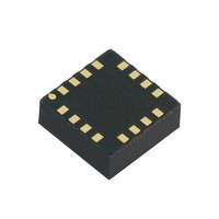
... LGA-16 (5x5x1.6mm) Land Grid Array Package 7887555A LY530AL ...
Page 29
... LY530AL 8 Revision history Table 33. Document revision history Date 03-Sep-2008 Revision 1 Initial release Revision history Changes 29/30 ...
Page 30
... Australia - Belgium - Brazil - Canada - China - Czech Republic - Finland - France - Germany - Hong Kong - India - Israel - Italy - Japan - Malaysia - Malta - Morocco - Singapore - Spain - Sweden - Switzerland - United Kingdom - United States of America 30/30 Please Read Carefully: © 2008 STMicroelectronics - All rights reserved STMicroelectronics group of companies www.st.com LY530AL ...