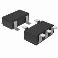
BD7411G-TR Rohm Semiconductor, BD7411G-TR Datasheet - Page 23

BD7411G-TR
Manufacturer Part Number
BD7411G-TR
Description
IC OMNI DETECTION 5.5V SSOP-5
Manufacturer
Rohm Semiconductor
Type
Omnipolar Switchr
Series
-r
Specifications of BD7411G-TR
Sensing Range
±5.6mT Trip, ±1.5mT Release
Voltage - Supply
4.5 V ~ 5.5 V
Current - Supply
4mA
Current - Output (max)
±1mA
Output Type
Digital, Open Collector
Operating Temperature
-40°C ~ 85°C
Package / Case
6-LSOP (0.063", 1.6mm Width) 5 Leads
Hall Effect Type
Unipolar
Output Current
1mA
Power Dissipation Pd
540mW
Sensor Case Style
SSOP
No. Of Pins
5
Supply Voltage Range
4.5V To 5.5V
Operating Temperature Range
-40°C To +85°C
Svhc
No SVHC
Base Number
7411
Rohs Compliant
Yes
Features
-
Lead Free Status / RoHS Status
Lead free / RoHS Compliant
Features
-
Lead Free Status / Rohs Status
Lead free / RoHS Compliant
Available stocks
Company
Part Number
Manufacturer
Quantity
Price
Company:
Part Number:
BD7411G-TR
Manufacturer:
BOURNS
Quantity:
66 000
●Description of Operations
© 2010 ROHM Co., Ltd. All rights reserved.
BU52001GUL,BU52011HFV,BU52021HFV,BU52015GUL,BU52025G,BU52051NVX,
BU52053NVX,BU52054GWZ,BU52055GWZ,BU52056NVX,BU52061NVX,BD7411G
www.rohm.com
I
(Offset Cancelation)
DD
(Micropower Operation)
B
GND
Fig.66
V
Startup time
×
DD
Standby time
Period
Fig.65
I
+
-
Hall Voltage
t
The bipolar detection Hall IC adopts an intermittent operation method
to save energy. At startup, the Hall elements, amp, comparator and
other detection circuits power ON and magnetic detection begins.
During standby, the detection circuits power OFF, thereby reducing
current consumption. The detection results are held while standby is
active, and then output.
Reference period: 50ms (MAX100ms)
Reference startup time: 48µs
※BD7411G don’t adopts an intermittent operation method.
The Hall elements form an equivalent Wheatstone (resistor) bridge
circuit. Offset voltage may be generated by a differential in this bridge
resistance, or can arise from changes in resistance due to package or
bonding stress. A dynamic offset cancellation circuit is employed to
cancel this offset voltage.
When Hall elements are connected as shown in Fig. 66 and a
magnetic field is applied perpendicular to the Hall elements, voltage is
generated at the mid-point terminal of the bridge. This is known as Hall
voltage.
Dynamic cancellation switches the wiring (shown in the figure) to
redirect the current flow to a 90˚ angle from its original path, and
thereby cancels the Hall voltage.
The magnetic signal (only) is maintained in the sample/hold circuit
during the offset cancellation process and then released.
23/31
Technical Note
2010.12 - Rev.F


