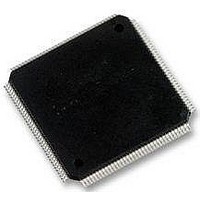
STM32F103ZGH6 STMicroelectronics, STM32F103ZGH6 Datasheet - Page 90

STM32F103ZGH6
Manufacturer Part Number
STM32F103ZGH6
Description
MCU 32BIT 1MB FLASH 144LQFP
Manufacturer
STMicroelectronics
Series
STM32r
Datasheet
1.STM32F103VGT6.pdf
(120 pages)
Specifications of STM32F103ZGH6
Core Processor
ARM® Cortex-M3™
Core Size
32-Bit
Speed
72MHz
Connectivity
CAN, I²C, IrDA, LIN, MMC, SPI, UART/USART, USB
Peripherals
DMA, I²S, LCD, POR, PWM, WDT
Number Of I /o
112
Program Memory Size
1MB (1M x 8)
Program Memory Type
FLASH
Ram Size
96K x 8
Voltage - Supply (vcc/vdd)
2 V ~ 3.6 V
Data Converters
A/D 21x12b; D/A 2x12b
Oscillator Type
Internal
Operating Temperature
-40°C ~ 85°C
Package / Case
*
Processor Series
STM32F101xG
Core
ARM Cortex M3
Data Bus Width
32 bit
Data Ram Size
80 KB
Interface Type
I2C, SPI, UART
Maximum Clock Frequency
36 MHz
Number Of Programmable I/os
112
Number Of Timers
15
Operating Supply Voltage
2 V to 3.6 V
Maximum Operating Temperature
+ 85 C
Mounting Style
SMD/SMT
Operating Temperature Range
- 40 C to + 105 C
Processor To Be Evaluated
STM32F103ZG
Supply Current (max)
28 mA
Lead Free Status / RoHS Status
Lead free / RoHS Compliant
Eeprom Size
-
Lead Free Status / Rohs Status
Details
Other names
497-11115
Available stocks
Company
Part Number
Manufacturer
Quantity
Price
Company:
Part Number:
STM32F103ZGH6
Manufacturer:
STMicroelectronics
Quantity:
135
Company:
Part Number:
STM32F103ZGH6
Manufacturer:
STMicroelectronics
Quantity:
10 000
Part Number:
STM32F103ZGH6
Manufacturer:
ST
Quantity:
20 000
Electrical characteristics
5.3.15
90/120
Figure 44. I/O AC characteristics definition
NRST pin characteristics
The NRST pin input driver uses CMOS technology. It is connected to a permanent pull-up
resistor, R
Unless otherwise specified, the parameters given in
performed under ambient temperature and V
Table
Table 49.
1. Guaranteed by design, not tested in production.
2. The pull-up is designed with a true resistance in series with a switchable PMOS. This PMOS contribution
Figure 45. Recommended NRST pin protection
2. The reset network protects the device against parasitic resets.
3. The user must ensure that the level on the NRST pin can go below the V
V
V
V
V
V
NF(NRST)
IH(NRST)
IL(NRST)
Symbol
F(NRST)
hys(NRST)
to the series resistance must be minimum
Table
R
10.
PU
49. Otherwise the reset will not be taken into account by the device.
(1)
(1)
(1)
(1)
PU
External
reset circuit
NRST pin characteristics
(see
NRST Input low level voltage
NRST Input high level voltage
NRST Schmitt trigger voltage
hysteresis
Weak pull-up equivalent resistor
NRST Input filtered pulse
NRST Input not filtered pulse
EXT ERNAL
OUTPUT
ON 50pF
Maximum frequency is achieved if (t r + t f ) 2/3)T and if the duty cycle is (45-55%)
Table
(1)
0.1 µF
46).
Parameter
t r(I O)out
NRST
(2)
Doc ID 16554 Rev 2
(~10% order)
10%
V DD
50%
when loaded by 50pF
R PU
90%
(2)
.
DD
supply voltage conditions summarized in
Conditions
V
T
10%
IN
Table 49
50%
V
Filter
SS
90%
t r(I O)out
STM32F103xF, STM32F103xG
STM32F10xxx
are derived from tests
IL(NRST)
Internal Reset
–0.5
Min
300
30
2
max level specified in
Typ
200
40
V
ai14132d
DD
Max
100
0.8
50
+0.5
ai14131
Unit
mV
k
ns
ns
V


