PD57006 STMicroelectronics, PD57006 Datasheet
PD57006
Specifications of PD57006
Available stocks


Related parts for PD57006


PD57006 Summary of contents
Page 1
... It is designed for high gain, broad band commercial and industrial applications. It operates common source mode at frequencies GHz. PD57006 boasts the excellent gain, linearity and reliability of ST’s latest LDMOS technology mounted in the first true SMD plastic RF power package, PowerSO-10RF. Device’s superior linearity performance makes it an ideal solution for car mobile radio ...
Page 2
... Thermal data . . . . . . . . . . . . . . . . . . . . . . . . . . . . . . . . . . . . . . . . . . . . . . . 3 2 Electrical characteristics . . . . . . . . . . . . . . . . . . . . . . . . . . . . . . . . . . . . . 4 2.1 Static . . . . . . . . . . . . . . . . . . . . . . . . . . . . . . . . . . . . . . . . . . . . . . . . . . . . . 4 2.2 Dynamic . . . . . . . . . . . . . . . . . . . . . . . . . . . . . . . . . . . . . . . . . . . . . . . . . . . 4 2.3 Moisture sensitivity level . . . . . . . . . . . . . . . . . . . . . . . . . . . . . . . . . . . . . . . 4 3 Impedance . . . . . . . . . . . . . . . . . . . . . . . . . . . . . . . . . . . . . . . . . . . . . . . . . 5 4 Typical performance . . . . . . . . . . . . . . . . . . . . . . . . . . . . . . . . . . . . . . . . . 6 4.1 PD57006 4.2 PD5706S Test circuit . . . . . . . . . . . . . . . . . . . . . . . . . . . . . . . . . . . . . . . . . . . . . . . . 12 6 Common source s-parameter . . . . . . . . . . . . . . . . . . . . . . . . . . . . . . . . 14 7 Package mechanical data . . . . . . . . . . . . . . . . . . . . . . . . . . . . . . . . . . . . 16 8 Revision history . . . . . . . . . . . . . . . . . . . . . . . . . . . . . . . . . . . . . . . . . . . 21 2/22 Doc ID 12611 Rev 2 PD57006-E, PD57006S-E ...
Page 3
... PD57006-E, PD57006S-E 1 Electrical data 1.1 Maximum ratings Table 2. Absolute maximum ratings (T Symbol V (BR)DSS DISS STG 1.2 Thermal data Table 3. Thermal data Symbol R thJC CASE Parameter Drain-source voltage Gate-source voltage Drain current Power dissipation (@ T = 70°C) C Max. operating junction temperature Storage temperature ...
Page 4
... MHz MHz MHz DS Test conditions 945 MHz 945 MHz DQ OUT 945 MHz DQ OUT 945 MHz DQ OUT Test methodology J-STD-020B Doc ID 12611 Rev 2 PD57006-E, PD57006S-E Min Typ Max Unit 65 μA 1 μA 1 2.0 5.0 V 0.9 V 0.58 mho 0.9 pF Min Typ Max Unit 10:1 ...
Page 5
... PD57006-E, PD57006S-E 3 Impedance Figure 2. Current conventions Table 7. Impedance data Freq. (MHz) 925 6.040 - j 0.936 945 5.886 - j 2.326 960 6.056 - j 3.522 PD57006 Z (Ω) Z (Ω) Freq. (MHz 6.273 + j 8.729 6.578 + j 5.999 7.215 + j 7.539 Doc ID 12611 Rev 2 Impedance PD57006S Z (Ω 925 3.794 - j 1.632 3.513 + j 10.81 945 4 ...
Page 6
... VDD, DRAIN VOLTAGE (V) Figure 5. Gate-source voltage vs case temperature 1.06 1.04 1.02 1 0.98 0.96 Vds=10 V 0.94 0.92 - Tc, CASE TEMPERATURE (°C) 6/22 Figure 4. C iss C oss C rss Id=1.5 A Id=1 A Id=.6 A Id=.2 A Id=. 100 Doc ID 12611 Rev 2 PD57006-E, PD57006S-E Drain current vs gate source voltage ...
Page 7
... PD57006-E, PD57006S-E 4.1 PD57006-E Figure 6. Output power vs input power 9 8 925 MHz 960 MHz 0.1 0.2 Pin, INPUT POWER (W) Figure 8. Power gain vs output power 945 MHz Pout, OUTPUT POWER (W) Figure 945 MHz -10 -15 Vdd=28V -20 Idq=70mA -25 0.3 0 Figure 9. 60 925 MHz 50 960 MHz ...
Page 8
... MHz 40 960 MHz 30 20 Idq=70 mA Pin= 23.6 dBm Doc ID 12611 Rev 2 PD57006-E, PD57006S-E 945 MHz 925 MHz 960 MHz Vdd=28V Pin= 23.6 dBm 100 200 300 IDQ, BIAS CURRENT (mA) 925 MHz 945 MHz 960 MHz Idq Pin= 23.6 dBm 12 14 ...
Page 9
... PD57006-E, PD57006S-E Figure 14. Output power vs gate-source voltage VGS, GATE-SOURCE VOLTAGE (V) 4.2 PD5706S-E Figure 15. Output power vs input power 9 8 925 945 0.1 0.2 Pin, INPUT POWER (W) 925 MHz 960 MHz 945 MHz Vdd=28V Pin= 23.6 dBm 3 4 Figure 16. Input return loss vs output power ...
Page 10
... Figure 18. Drain efficiency vs output power 60 925 960 Figure 20. Drain efficiency vs bias current dd=28V 22 300 400 0 Doc ID 12611 Rev 2 PD57006-E, PD57006S-E 945 960 925 dd=28V Idq=70m Pout, OUTPUT POWER (W) 945 925 960 Vdd=28V Pin = 22.7 dBm 100 200 300 IDQ, BIAS CURRENT (mA 400 ...
Page 11
... PD57006-E, PD57006S-E Figure 21. Output power vs supply voltage 945 VDD, SUPPLY VOLTAGE (V) Figure 23. Output power vs gate-source voltage 945 VGS, GATE-SOURCE VOLTAGE (V) Figure 22. Drain efficiency vs supply voltage 60 925 960 22 925 960 dd=28V P in= 22 Doc ID 12611 Rev 2 Typical performance 960 925 945 Idq= 22 VDD, SUPPLY VOLTAGE (V) ...
Page 12
... BOARD Doc ID 12611 Rev 2 PD57006-E, PD57006S-E 18 kΩ CHIP RESISTOR 1 W 4.7 mΩ CHIP RESISTOR kΩ CHIP RESISTOR 1 W 0.430” X 0.084” MICROSTRIP 0.1.186” X 1.120” MICROSTRIP 1.273” X 0.565” MICROSTRIP 0.770” X 0.171” MICROSTRIP 0.880” X 0.105” MICROSTRIP 1.200” ...
Page 13
... PD57006-E, PD57006S-E Figure 25. Test circuit photomaster Figure 26. Test circuit Table 9. Transmission line dimensions 0.430” X 0.084” Z1 MICROSTRIP 0.220” X 0.155” Z2 MICROSTRIP 0.960” X 0.120” Z3 MICROSTRIP 6.4 inches 1.273” X 0.565” Z4 MICROSTRIP 0.195” X 0.250” Z5 MICROSTRIP 0.555” X 0.171” ...
Page 14
... Common source s-parameter 6 Common source s-parameter Table 10. S-parameter for PD57006-E (V Freq < Φ (MHz) 50 0.895 -79 100 0.786 -118 150 0.765 -134 200 0.767 -143 250 0.778 -151 300 0.790 -156 350 0.794 -159 400 0.806 -162 450 0.814 -165 500 0.826 -167 550 0 ...
Page 15
... PD57006-E, PD57006S-E Table 11. S-parameter PD57006-E (V Freq < Φ (MHz) 50 0.953 -65 100 0.855 -104 150 0.823 -124 200 0.818 -136 250 0.824 -144 300 0.832 -150 350 0.835 -155 400 0.845 -159 450 0.850 -162 500 0.860 -165 550 0.866 -168 600 0.870 ...
Page 16
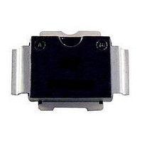
... Package mechanical data 7 Package mechanical data In order to meet environmental requirements, ST offers these devices in different grades of ® ECOPACK packages, depending on their level of environmental compliance. ECOPACK specifications, grade definitions and product status are available at: www.st.com. ® ECOPACK trademark. 16/22 Doc ID 12611 Rev 2 PD57006-E, PD57006S-E ® ...
Page 17
... PD57006-E, PD57006S-E Table 12. PowerSO-10RF formed lead (Gull Wing) mechanical data Dim Note: Resin protrusions not included (max value: 0.15 mm per side) Figure 27. Package dimensions mm. Min. Typ. Max. 0 0.05 0.1 3.4 3.5 3.6 1.2 1.3 1.4 0.15 0.2 0.25 0.2 5.4 5.53 5 ...
Page 18
... Doc ID 12611 Rev 2 PD57006-E, PD57006S-E Inch Min. Typ. Max. 0.064 0.065 0.068 0.134 0.137 0.142 0.046 0.05 0.054 0.005 0.007 0.009 0.007 0.212 ...
Page 19
... PD57006-E, PD57006S-E Figure 29. Tube information Doc ID 12611 Rev 2 Package mechanical data 19/22 ...
Page 20
... Package mechanical data Figure 30. Reel information 20/22 Doc ID 12611 Rev 2 PD57006-E, PD57006S-E ...
Page 21
... PD57006-E, PD57006S-E 8 Revision history Table 14. Document revision history Date 06-May-2006 25-May-2010 Revision 1 Initial release. 2 Added: Table 6: Moisture sensitivity Doc ID 12611 Rev 2 Revision history Changes level. 21/22 ...
Page 22
... Australia - Belgium - Brazil - Canada - China - Czech Republic - Finland - France - Germany - Hong Kong - India - Israel - Italy - Japan - Malaysia - Malta - Morocco - Philippines - Singapore - Spain - Sweden - Switzerland - United Kingdom - United States of America 22/22 Please Read Carefully: © 2010 STMicroelectronics - All rights reserved STMicroelectronics group of companies www.st.com Doc ID 12611 Rev 2 PD57006-E, PD57006S-E ...