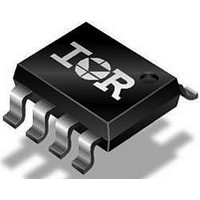
IRF7410PBF International Rectifier, IRF7410PBF Datasheet - Page 2

IRF7410PBF
Manufacturer Part Number
IRF7410PBF
Description
P CHANNEL MOSFET, -12V, 16A, SOIC
Manufacturer
International Rectifier
Specifications of IRF7410PBF
Transistor Polarity
P Channel
Continuous Drain Current Id
-16A
Drain Source Voltage Vds
-12V
On Resistance Rds(on)
7mohm
Rds(on) Test Voltage Vgs
-4.5V
Threshold Voltage Vgs Typ
-900mV
Channel Type
P
Current, Drain
-16 A
Gate Charge, Total
91 nC
Package Type
SO-8
Polarization
P-Channel
Power Dissipation
2.5 W
Resistance, Drain To Source On
7 Milliohms
Temperature, Operating, Maximum
+150 °C
Temperature, Operating, Minimum
-55 °C
Time, Turn-off Delay
271 ns
Time, Turn-on Delay
13 ns
Transconductance, Forward
55 S
Voltage, Breakdown, Drain To Source
-12 V
Voltage, Drain To Source
–12 V
Voltage, Forward, Diode
-1.2 V
Voltage, Gate To Source
±8 V
Lead Free Status / RoHS Status
Lead free / RoHS Compliant
Lead Free Status / RoHS Status
Lead free / RoHS Compliant
Notes:
‚
V
∆V
R
V
∆V
gfs
I
I
Q
Q
Q
t
t
t
t
C
C
C
I
I
V
t
Q
Electrical Characteristics @ TJ = 25°C (unless otherwise specified)
Source-Drain Ratings and Characteristics
DSS
GSS
d(on)
r
d(off)
f
S
SM
rr
(BR)DSS
GS(th)
SD
DS(on)
g
gs
gd
iss
oss
rss
rr
2
Symbol
Symbol
Repetitive rating; pulse width limited by
Pulse width ≤ 400µs; duty cycle ≤ 2%.
(BR)DSS
GS(th)
max. junction temperature.
/∆T
/∆T
J
J
Drain-to-Source Breakdown Voltage
Breakdown Voltage Temp. Coefficient
Static Drain-to-Source On-Resistance
Gate Threshold Voltage
Gate Threshold Voltage Coefficient
Forward Transconductance
Drain-to-Source Leakage Current
Gate-to-Source Forward Leakage
Gate-to-Source Reverse Leakage
Total Gate Charge
Gate-to-Source Charge
Gate-to-Drain ("Miller") Charge
Turn-On Delay Time
Rise Time
Turn-Off Delay Time
Fall Time
Input Capacitance
Output Capacitance
Reverse Transfer Capacitance
Continuous Source Current
(Body Diode)
Pulsed Source Current
(Body Diode)
Diode Forward Voltage
Reverse Recovery Time
Reverse Recovery Charge
Parameter
Parameter
™
ƒ
Surface mounted on 1 in square Cu board, t ≤ 10sec.
Min.
Min.
–––
–––
–––
–––
-0.4
–––
–––
–––
–––
–––
–––
–––
–––
–––
–––
–––
–––
–––
–––
–––
–––
–––
–––
–––
–––
-12
55
0.006
Typ. Max. Units
8676
2344
1604
Typ. Max. Units
-3.09
–––
–––
–––
–––
–––
–––
–––
–––
–––
–––
271
200
–––
–––
–––
134
91
18
25
13
12
97
-100
–––
–––
-0.9
–––
–––
-1.0
100
–––
407
300
–––
–––
–––
-2.5
-1.2
145
201
-25
-65
13
20
18
7
9
mV/°C
V/°C
mΩ
µA
nA
nC
µC
pF
ns
ns
V
V
S
A
V
V
Reference to 25°C, I
V
V
V
V
V
V
V
V
V
I
V
V
V
I
R
R
V
V
ƒ = 1.0 MHz
MOSFET symbol
showing the
integral reverse
p-n junction diode.
T
T
di/dt = -100A/µs
D
D
J
J
GS
GS
GS
GS
DS
DS
DS
DS
GS
GS
DS
GS
DD
D
G
GS
DS
= -16A
=-1.0A
= 25°C, I
= 25°C
= 6Ω
= 6Ω
= V
= -10V, I
= -9.6V, V
= -9.6V, V
=-9.6V
= -10V
= 0V, I
= -4.5V, I
= -2.5V, I
= -1.8V, I
= -8V
= 8V
= -4.5V
= -6V V
= 0V
GS
d
, I
Conditions
Conditions
D
S
D
d
= -250µA
D
GS
= -2.5A, V
D
D
D
= -250µA
GS
GS
= -16A
= -16A
= -13.6A
= -11.5A
= -4.5V
www.irf.com
d
= 0V
= 0V, T
G
I
D
F
= -2.5A
= -1mA
d
GS
d
d
J
= 70°C
= 0V
D
S
d


