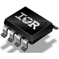
IRF7410PBF International Rectifier, IRF7410PBF Datasheet - Page 3

IRF7410PBF
Manufacturer Part Number
IRF7410PBF
Description
P CHANNEL MOSFET, -12V, 16A, SOIC
Manufacturer
International Rectifier
Specifications of IRF7410PBF
Transistor Polarity
P Channel
Continuous Drain Current Id
-16A
Drain Source Voltage Vds
-12V
On Resistance Rds(on)
7mohm
Rds(on) Test Voltage Vgs
-4.5V
Threshold Voltage Vgs Typ
-900mV
Channel Type
P
Current, Drain
-16 A
Gate Charge, Total
91 nC
Package Type
SO-8
Polarization
P-Channel
Power Dissipation
2.5 W
Resistance, Drain To Source On
7 Milliohms
Temperature, Operating, Maximum
+150 °C
Temperature, Operating, Minimum
-55 °C
Time, Turn-off Delay
271 ns
Time, Turn-on Delay
13 ns
Transconductance, Forward
55 S
Voltage, Breakdown, Drain To Source
-12 V
Voltage, Drain To Source
–12 V
Voltage, Forward, Diode
-1.2 V
Voltage, Gate To Source
±8 V
Lead Free Status / RoHS Status
Lead free / RoHS Compliant
Lead Free Status / RoHS Status
Lead free / RoHS Compliant
www.irf.com
Fig 3. Typical Transfer Characteristics
0.01
Fig 1. Typical Output Characteristics
100
100
0.1
0.1
10
10
1
1
0.2
0.1
T J = 150°C
0.4
V DS , Drain-to-Source Voltage (V)
V GS , Gate-to-Source Voltage (V)
0.6
≤ 60µs PULSE WIDTH
Tj = 25°C
1
0.8
-1.0V
V DS = -10V
≤60µs PULSE WIDTH
1
T J = 25°C
1.2
10
TOP
BOTTOM
1.4
1.6
VGS
-7.0V
-5.0V
-4.5V
-2.5V
-1.8V
-1.5V
-1.2V
-1.0V
100
1.8
100
10
2.0
1.5
1.0
0.5
0.0
1
0.1
Fig 4. Normalized On-Resistance
-60 -40 -20
Fig 2. Typical Output Characteristics
I =
D
-16A
V DS , Drain-to-Source Voltage (V)
T , Junction Temperature ( C)
J
Vs. Temperature
0
1
-1.0V
20 40 60 80 100 120 140 160
≤ 60µs PULSE WIDTH
Tj = 150°C
10
TOP
BOTTOM
V
GS
°
VGS
-7.0V
-5.0V
-4.5V
-2.5V
-1.8V
-1.5V
-1.2V
-1.0V
=
-4.5V
3
100


