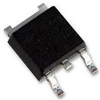
NID5001N
Self−Protected FET
with Temperature and
Current Limit
utilize ON Semicondutor’s latest MOSFET technology process to
achieve the lowest possible on−resistance per silicon area while
incorporating smart features. Integrated thermal and current limits
work together to provide short circuit protection. The devices feature
an integrated Drain−to−Gate Clamp that enables them to withstand
high energy in the avalanche mode. The Clamp also provides
additional safety margin against unexpected voltage transients.
Electrostatic Discharge (ESD) protection is provided by an integrated
Gate−to−Source Clamp.
Features
•
•
•
•
•
•
•
•
•
Stresses exceeding Maximum Ratings may damage the device. Maximum
Ratings are stress ratings only. Functional operation above the Recommended
Operating Conditions is not implied. Extended exposure to stresses above the
Recommended Operating Conditions may affect device reliability.
1. Minimum FR4 PCB, steady state.
2. Mounted onto a 2″ square FR4 board
MAXIMUM RATINGS
© Semiconductor Components Industries, LLC, 2006
April, 2006 − Rev. 8
Drain−to−Source Voltage Internally Clamped
Drain−to−Gate Voltage Internally Clamped
Gate−to−Source Voltage
Drain Current − Continuous
Total Power Dissipation
Thermal Resistance, Junction−to−Case
Single Pulse Drain−to−Source Avalanche
Energy
Operating and Storage Temperature Range
HDPlus devices are an advanced series of power MOSFETs which
Low R
Current Limitation
Thermal Shutdown with Automatic Restart
Short Circuit Protection
I
Avalanche Energy Specified
Slew Rate Control for Low Noise Switching
Overvoltage Clamped Protection
Pb−Free Package is Available
(1″ square, 2 oz. Cu 0.06″ thick single−sided, t = steady state).
DSS
(R
@ T
@ T
@ T
Junction−to−Ambient (Note 1)
Junction−to−Ambient (Note 2)
(V
I
L
GS
DD
= 4.5 Apk, L = 120 mH, R
Specified at Elevated Temperature
A
A
A
= 25 Vdc, V
= 1.0 MW)
DS(on)
= 25°C (Note 1)
= 25°C (Note 1)
= 25°C (Note 2)
Rating
GS
(T
= 5.0 Vdc,
J
= 25°C unless otherwise noted)
G
= 25 W)
Symbol
T
V
V
R
R
R
J
V
E
P
DGR
, T
DSS
I
qJC
qJA
qJA
GS
AS
D
D
stg
−55 to 150
Internally Limited
Value
"14
1215
1.56
1.95
120
1.0
42
42
64
80
1
°C/W
Unit
Vdc
Vdc
Vdc
mJ
°C
W
*Max current may be limited below this value
Y
WW
D5001N = Device Code
G
†For information on tape and reel specifications,
Gate
Input
NID5001NT4
NID5001NT4G
depending on input conditions.
including part orientation and tape sizes, please
refer to our Tape and Reel Packaging Specification
Brochure, BRD8011/D.
(Clamped)
V
CASE 369C
42 V
Device
DSS
STYLE 2
ESD Protection
DPAK
= Year
= Work Week
= Pb−Free Package
ORDERING INFORMATION
Temperature
R
G
http://onsemi.com
Limit
23 mW @ 10 V
R
Overvoltage
(Pb−Free)
Protection
Package
DS(ON)
DPAK
DPAK
Publication Order Number:
TYP
Current
Limit
1
3
2500/Tape & Reel
2500/Tape & Reel
2
1 = Gate
2 = Drain
3 = Source
Shipping
MARKING
DIAGRAM
Drain
NID5001N/D
(Limited)
Current
Sense
I
Source
YWW
01NG
D
33 A*
D50
MAX
M
†
PWR


