TFBS6711-TR1 Vishay, TFBS6711-TR1 Datasheet - Page 2
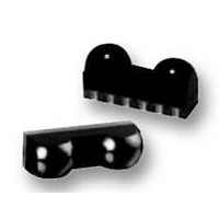
TFBS6711-TR1
Manufacturer Part Number
TFBS6711-TR1
Description
IRDA FIR TRANSCEIVER 1,9MM-e4
Manufacturer
Vishay
Datasheet
1.TFBS6711-TR1.pdf
(14 pages)
Specifications of TFBS6711-TR1
Data Rate Max
4Mbps
Data Transmission Distance
30cm
Peak Wavelength
900nm
Supply Current
1.9mA
Supply Voltage Range
2.4V To 3.6V
Operating Temperature Range
-25°C To +85°C
Msl
MSL 4 - 72 Hours
External
RoHS Compliant
External Depth
1.9mm
Rohs Compliant
Yes
Current Ilireda
1µA
Svhc
No SVHC (20-Jun-2011)
Lead Free Status / RoHS Status
Available stocks
Company
Part Number
Manufacturer
Quantity
Price
Company:

Part Number:
TFBS6711-TR1
Manufacturer:
ACTEL
Quantity:
1 200
Company:
Part Number:
TFBS6711-TR1
Manufacturer:
VISHAY
Quantity:
398


Functional Block Diagram
Pin Description
TFBS6711
Weight: 50 mg
Document Number 84676
Rev. 1.2, 03-Jul-06
Pin Number
1
2
3
4
5
6
19298
V
Function
CC2
TXD
SD
Anode
V
GND
TXD
RXD
SD
CC1
, IRED
3.6 V an external resistor might be necessary for reducing the internal power
dissipation. See derating curves. This pin is allowed to be supplied from an
standard CMOS load. No external pull-up or pull-down resistor is required.
Received Data Output, push-pull CMOS driver output capable of driving a
Floating with a weak pull-up of 500 kΩ (typ.) in shutdown mode. The RXD
IRED anode to be externally connected to V
uncontrolled power supply separated from the controlled V
Amplifier
Shutdown, also used for dynamic mode switching
output echos the TXD input during transmission.
Figure 1. Functional Block Diagramm
Comparator
Logic
&
Control
Transmit Data Input
Figure 2. Pinning
Supply voltage
GND
Description
PIN 1
Ground
V
CC1
CC2
. For higher voltages as
Controlled
Driver
19428
Tri-State
Driver
CC1
- supply
Vishay Semiconductors
V
RXD
CC2
I/O
O
I
I
TFBS6711
www.vishay.com
Active
HIGH
HIGH
LOW
259
Related parts for TFBS6711-TR1
Image
Part Number
Description
Manufacturer
Datasheet
Request
R

Part Number:
Description:
IRDA TRANSCEIVER FIR TRANSCEIVER 1
Manufacturer:
Vishay
Datasheet:

Part Number:
Description:
Infrared Transceivers FIR 4Mbit/s 2.4-3.6V Op Voltage
Manufacturer:
Vishay
Datasheet:
Part Number:
Description:
Low Profile Fast Infrared Transceiver Fir, 4 Mbit/s For Irda Applications
Manufacturer:
Vishay
Datasheet:
Part Number:
Description:
357-036-542-201 CARDEDGE 36POS DL .156 BLK LOPRO
Manufacturer:
Vishay
Datasheet:
Part Number:
Description:
357-036-542-201 CARDEDGE 36POS DL .156 BLK LOPRO
Manufacturer:
Vishay
Datasheet:
Part Number:
Description:
357-036-542-201 CARDEDGE 36POS DL .156 BLK LOPRO
Manufacturer:
Vishay
Datasheet:
Part Number:
Description:
357-036-542-201 CARDEDGE 36POS DL .156 BLK LOPRO
Manufacturer:
Vishay
Datasheet:
Part Number:
Description:
357-036-542-201 CARDEDGE 36POS DL .156 BLK LOPRO
Manufacturer:
Vishay
Datasheet:
Part Number:
Description:
357-036-542-201 CARDEDGE 36POS DL .156 BLK LOPRO
Manufacturer:
Vishay
Datasheet:
Part Number:
Description:
357-036-542-201 CARDEDGE 36POS DL .156 BLK LOPRO
Manufacturer:
Vishay
Datasheet:
Part Number:
Description:
357-036-542-201 CARDEDGE 36POS DL .156 BLK LOPRO
Manufacturer:
Vishay
Datasheet:
Part Number:
Description:
357-036-542-201 CARDEDGE 36POS DL .156 BLK LOPRO
Manufacturer:
Vishay
Datasheet:
Part Number:
Description:
357-036-542-201 CARDEDGE 36POS DL .156 BLK LOPRO
Manufacturer:
Vishay
Datasheet:
Part Number:
Description:
357-036-542-201 CARDEDGE 36POS DL .156 BLK LOPRO
Manufacturer:
Vishay
Datasheet:
Part Number:
Description:
357-036-542-201 CARDEDGE 36POS DL .156 BLK LOPRO
Manufacturer:
Vishay
Datasheet: