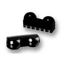
TFBS6711-TR1 Vishay, TFBS6711-TR1 Datasheet - Page 7

TFBS6711-TR1
Manufacturer Part Number
TFBS6711-TR1
Description
IRDA FIR TRANSCEIVER 1,9MM-e4
Manufacturer
Vishay
Datasheet
1.TFBS6711-TR1.pdf
(14 pages)
Specifications of TFBS6711-TR1
Data Rate Max
4Mbps
Data Transmission Distance
30cm
Peak Wavelength
900nm
Supply Current
1.9mA
Supply Voltage Range
2.4V To 3.6V
Operating Temperature Range
-25°C To +85°C
Msl
MSL 4 - 72 Hours
External
RoHS Compliant
External Depth
1.9mm
Rohs Compliant
Yes
Current Ilireda
1µA
Svhc
No SVHC (20-Jun-2011)
Lead Free Status / RoHS Status
Available stocks
Company
Part Number
Manufacturer
Quantity
Price
Company:
Part Number:
TFBS6711-TR1
Manufacturer:
ACTEL
Quantity:
1 200
Company:
Part Number:
TFBS6711-TR1
Manufacturer:
VISHAY
Quantity:
398
TFBS6711
Vishay Semiconductors
Recommended Circuit Diagram
Operated at a clean low impedance power supply the
TFBS6711 needs no additional external components.
However, depending on the entire system design and
board layout, additional components may be required
(see figure 3).
The capacitor C1 is buffering the supply voltage and
eliminates the inductance of the power supply line.
This one should be a Tantalum or other fast capacitor
to guarantee the fast rise time of the IRED current.
Vishay transceivers integrate a sensitive receiver and
a built-in power driver. The combination of both needs
a careful circuit board layout. The use of thin, long,
resistive and inductive wiring should be avoided. The
inputs (RXD, SD) and the output RXD should be
directly (DC) coupled to the I/O circuit.
The capacitor C2 combined with the resistor R2 is the
low pass filter for smoothing the supply voltage.
R2, C1 and C2 are optional and dependent on the
quality of the supply voltages V
noise. An unstable power supply with dropping volt-
age during transmission may reduce the sensitivity
(and transmission range) of the transceiver.
The placement of these parts is critical. It is strongly
recommended to position C2 as close as possible to
the transceiver power supply pins.
A Tantalum capacitor should be used for C1 while a
ceramic capacitor is used for C2.
www.vishay.com
264
19299
SD
TXD
RXD
V
V
GND
Figure 3. Recommended Application Circuit
CC2
CC1
C1
R2
C3
R1
C2
SD
TXD
RXD
IRED Anode
V
Ground
CCx
CC
and injected
In addition, when connecting the described circuit to
the power supply, low impedance wiring should be
used.
When extended wiring is used the inductance of the
power supply can cause dynamically a voltage drop
at V
follow the fast current rise time. In that case another
4.7 µF (type, see table under C1) at V
ful.
Keep in mind that basic RF-design rules for circuit
design should be taken into account. Especially
longer signal lines should not be used without termi-
nation. See e.g. "The Art of Electronics" Paul Horo-
witz, Winfield Hill, 1989, Cambridge University Press,
ISBN: 0521370957.
Table 1. Recommended Application Circuit Compo-
nents
I/O and Software
In the description, already different I/Os are men-
tioned. Different combinations are tested and the
function verified with the special drivers available
from the I/O suppliers. In special cases refer to the I/
O manual, the Vishay application notes, or contact
directly Vishay Sales, Marketing or Application.
Component
CC2
C1
C2
R1
R2
. Often some power supplies are not able to
3.3 V supply voltage: no resistor is necessary,
the internal controller is able to control the
VJ1206 Y 104 J XXMT
Recommended Value
293D 475X9 016B
0.1 µF, Ceramic
4.7 Ω, 0.125 W
Vishay part#:
Vishay part#:
4.7 µF, 16 V
current
Document Number 84676
CC2
Rev. 1.2, 03-Jul-06
will be help-


