TFBS6711-TR1 Vishay, TFBS6711-TR1 Datasheet - Page 5
TFBS6711-TR1
Manufacturer Part Number
TFBS6711-TR1
Description
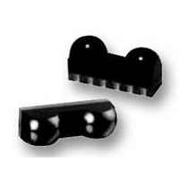
IRDA FIR TRANSCEIVER 1,9MM-e4
Manufacturer
Vishay
Datasheet
1.TFBS6711-TR1.pdf
(14 pages)
Specifications of TFBS6711-TR1
Data Rate Max
4Mbps
Data Transmission Distance
30cm
Peak Wavelength
900nm
Supply Current
1.9mA
Supply Voltage Range
2.4V To 3.6V
Operating Temperature Range
-25°C To +85°C
Msl
MSL 4 - 72 Hours
External
RoHS Compliant
External Depth
1.9mm
Rohs Compliant
Yes
Current Ilireda
1µA
Svhc
No SVHC (20-Jun-2011)
Lead Free Status / RoHS Status
Available stocks
Company
Part Number
Manufacturer
Quantity
Price
Company:

Part Number:
TFBS6711-TR1
Manufacturer:
ACTEL
Quantity:
1 200
Company:
Part Number:
TFBS6711-TR1
Manufacturer:
VISHAY
Quantity:
398


TFBS6711
Vishay Semiconductors
Optoelectronic Characteristics
T
Typical values are for DESIGN AID ONLY, not guaranteed nor subject to production testing.
Note: All timing data measured with 4 Mbit/s are measured using the IrDA
after starting the preamble.
**)
fication while the source is operating at the minimum intensity in angular range into the minimum half-angle range at the maximum Link
Length
***)
maximum intensity in angular range at Minimum Link Length must not cause receiver overdrive distortion and possible related link errors.
If placed at the Active Output Interface reference plane of the transmitter, the receiver must meet its bit error ratio (BER) specification.
For more definitions see the document “Symbols and Terminology” on the Vishay Website (http://www.vishay.com/docs/82512/82512.pdf).
www.vishay.com
262
Receiver
Minimum irradiance E
angular range **)
Minimum irradiance E
angular range
MIR mode
Minimum irradiance E
angular range
FIR mode
Maximum irradiance E
angular range ***)
No detection receiver Input
Irradiance (fluorescent light
noise suppression)
Rise time of output signal
Fall time of output signal
RXD pulse width of output
signal, 50%, SIR mode
RXD pulse width of output
signal, 50%, MIR mode
RXD pulse width of output
signal, 50%, FIR mode
RXD pulse width of output
signal, 50%, FIR mode
RXD output jitter, leading edge
Receiver start up time
Latency
amb
IrDA sensitivity definition: Minimum Irradiance E
Maximum Irradiance E
= 25 °C, V
Parameter
CC
= 2.4 V to 3.6 V unless otherwise noted.
e
e
e
e
in
in
in
in
e
In Angular Range, power per unit area. The optical delivered to the detector by a source operating at the
9.6 kbit/s to 115.2 kbit/s
1.152 Mbit/s
λ = 850 nm - 900 nm, V
4 Mbit/s
λ = 850 nm - 900 nm, V
λ = 850 nm - 900 nm
10 % to 90 %, C
90 % to 10 %, C
Input pulse length
1.4 μs < P
Input pulse length
P
Input pulse length
P
Input pulse length
P
Input irradiance = 150 mW/m
4 Mbit/s
1.152 Mbit/s
≤ 115.2 kbit/s
programming sequence
Power on delay
After completion of shutdown
λ = 850 nm - 900 nm, V
Wopt
Wopt
Wopt
= 217 ns, 1.152 Mbit/s
= 125 ns, 4 Mbit/s
= 250 ns, 4 Mbit/s
Test Conditions
Wopt
< 25 µs
L
L
= 15 pF
= 15 pF
e
In Angular Range, power per unit area. The receiver must meet the BER speci-
CC
CC
CC
= 2.4 V
= 2.4 V
= 2.4 V
2
,
®
Symbol
t
t
FIR transmission header. The data given here are valid 5 µs
r (RXD)
f (RXD)
t
t
t
t
E
E
E
E
E
PW
PW
PW
PW
t
L
e
e
e
e
e
(0.4)
110
110
225
Min
1.4
10
10
4
(500)
Typ.
(10)
(12)
100
120
250
1.8
(5)
50
5
Document Number 84676
Max
(20)
200
270
140
275
350
500
100
2.6
(8)
80
50
50
20
40
Rev. 1.2, 03-Jul-06
(mW/cm
(µW/cm
(µW/cm
(µW/cm
(µW/cm
mW/m
mW/m
mW/m
mW/m
kW/m
Unit
ns
ns
µs
ns
ns
ns
ns
ns
ns
µs
µs
2
2
2
2
2
2
2
2
2
2
)
)
)
)
)
Related parts for TFBS6711-TR1
Image
Part Number
Description
Manufacturer
Datasheet
Request
R

Part Number:
Description:
IRDA TRANSCEIVER FIR TRANSCEIVER 1
Manufacturer:
Vishay
Datasheet:

Part Number:
Description:
Infrared Transceivers FIR 4Mbit/s 2.4-3.6V Op Voltage
Manufacturer:
Vishay
Datasheet:
Part Number:
Description:
Low Profile Fast Infrared Transceiver Fir, 4 Mbit/s For Irda Applications
Manufacturer:
Vishay
Datasheet:
Part Number:
Description:
357-036-542-201 CARDEDGE 36POS DL .156 BLK LOPRO
Manufacturer:
Vishay
Datasheet:
Part Number:
Description:
357-036-542-201 CARDEDGE 36POS DL .156 BLK LOPRO
Manufacturer:
Vishay
Datasheet:
Part Number:
Description:
357-036-542-201 CARDEDGE 36POS DL .156 BLK LOPRO
Manufacturer:
Vishay
Datasheet:
Part Number:
Description:
357-036-542-201 CARDEDGE 36POS DL .156 BLK LOPRO
Manufacturer:
Vishay
Datasheet:
Part Number:
Description:
357-036-542-201 CARDEDGE 36POS DL .156 BLK LOPRO
Manufacturer:
Vishay
Datasheet:
Part Number:
Description:
357-036-542-201 CARDEDGE 36POS DL .156 BLK LOPRO
Manufacturer:
Vishay
Datasheet:
Part Number:
Description:
357-036-542-201 CARDEDGE 36POS DL .156 BLK LOPRO
Manufacturer:
Vishay
Datasheet:
Part Number:
Description:
357-036-542-201 CARDEDGE 36POS DL .156 BLK LOPRO
Manufacturer:
Vishay
Datasheet:
Part Number:
Description:
357-036-542-201 CARDEDGE 36POS DL .156 BLK LOPRO
Manufacturer:
Vishay
Datasheet:
Part Number:
Description:
357-036-542-201 CARDEDGE 36POS DL .156 BLK LOPRO
Manufacturer:
Vishay
Datasheet:
Part Number:
Description:
357-036-542-201 CARDEDGE 36POS DL .156 BLK LOPRO
Manufacturer:
Vishay
Datasheet:
Part Number:
Description:
357-036-542-201 CARDEDGE 36POS DL .156 BLK LOPRO
Manufacturer:
Vishay
Datasheet: