IP-SDRAM/DDR3 Altera, IP-SDRAM/DDR3 Datasheet
IP-SDRAM/DDR3
Specifications of IP-SDRAM/DDR3


Related parts for IP-SDRAM/DDR3


IP-SDRAM/DDR3 Summary of contents
Page 1
... External Memory Interface Handbook Volume 3 Section II. DDR3 SDRAM Controller with ALTMEMPHY IP User Guide External Memory Interface Handbook Volume 3 Section II. DDR3 SDRAM Controller with ALTMEMPHY IP 101 Innovation Drive San Jose, CA 95134 www.altera.com EMI_DDR3_UG-2.1 Document last updated for Altera Complete Design Suite version: ...
Page 2
... Altera. Altera customers are advised to obtain the latest version of device specifications before relying on any published information and before placing orders for products or services. External Memory Interface Handbook Volume 3 Section II. DDR3 SDRAM Controller with ALTMEMPHY IP User Guide December 2010 Altera Corporation ...
Page 3
... Specifying Parameters . . . . . . . . . . . . . . . . . . . . . . . . . . . . . . . . . . . . . . . . . . . . . . . . . . . . . . . . . . . . . . . . . 2–4 Generated Files . . . . . . . . . . . . . . . . . . . . . . . . . . . . . . . . . . . . . . . . . . . . . . . . . . . . . . . . . . . . . . . . . . . . . . . . . 2–6 HardCopy Device Migration Guidelines . . . . . . . . . . . . . . . . . . . . . . . . . . . . . . . . . . . . . . . . . . . . . . . . . . . 2–10 Enabling Hardcopy Migration Performance Improvement with ALTMEMPHY . . . . . . . . . . . . . . 2–10 Generating Your IP Core For a Mid-speed Grade FPGA . . . . . . . . . . . . . . . . . . . . . . . . . . . . . . . . 2–10 Compiling Your Design for a Faster Speed Grade FPGA . . . . . . . . . . . . . . . . . . . . . . . . . . . . . . . . 2–11 Chapter 3. Parameter Settings ALTMEMPHY Parameter Settings . . . . . . . . . . . . . . . . . . . . . . . . . . . . . . . . . . . . . . . . . . . . . . . . . . . . . . . . . 3–1 Memory Settings . . . . . . . . . . . . . . . . . . . . . . . . . . . . . . . . . . . . . . . . . . . . . . . . . . . . . . . . . . . . . . . . . . . . . . 3– ...
Page 4
... Timer Logic . . . . . . . . . . . . . . . . . . . . . . . . . . . . . . . . . . . . . . . . . . . . . . . . . . . . . . . . . . . . . . . . . . . . . . . . . . 6–3 Initialization State Machine . . . . . . . . . . . . . . . . . . . . . . . . . . . . . . . . . . . . . . . . . . . . . . . . . . . . . . . . . . . . . 6–3 Address and Command Decode . . . . . . . . . . . . . . . . . . . . . . . . . . . . . . . . . . . . . . . . . . . . . . . . . . . . . . . . 6–3 PHY Interface Logic . . . . . . . . . . . . . . . . . . . . . . . . . . . . . . . . . . . . . . . . . . . . . . . . . . . . . . . . . . . . . . . . . . . 6–4 ODT Generation Logic . . . . . . . . . . . . . . . . . . . . . . . . . . . . . . . . . . . . . . . . . . . . . . . . . . . . . . . . . . . . . . . . . 6–4 Low-Power Mode Logic . . . . . . . . . . . . . . . . . . . . . . . . . . . . . . . . . . . . . . . . . . . . . . . . . . . . . . . . . . . . . . . 6–4 External Memory Interface Handbook Volume 3 Section II. DDR3 SDRAM Controller with ALTMEMPHY IP User Guide Contents December 2010 Altera Corporation ...
Page 5
... Configuration and Status Register (CSR) Interface . . . . . . . . . . . . . . . . . . . . . . . . . . . . . . . . . . . . . . . . . 7–7 Error Correction Coding (ECC 7–7 Partial Writes . . . . . . . . . . . . . . . . . . . . . . . . . . . . . . . . . . . . . . . . . . . . . . . . . . . . . . . . . . . . . . . . . . . . . . 7–8 Partial Bursts . . . . . . . . . . . . . . . . . . . . . . . . . . . . . . . . . . . . . . . . . . . . . . . . . . . . . . . . . . . . . . . . . . . . . . . 7–9 Example Top-Level File . . . . . . . . . . . . . . . . . . . . . . . . . . . . . . . . . . . . . . . . . . . . . . . . . . . . . . . . . . . . . . . . . 7–10 Example Driver . . . . . . . . . . . . . . . . . . . . . . . . . . . . . . . . . . . . . . . . . . . . . . . . . . . . . . . . . . . . . . . . . . . . . . 7–11 Top-level Signals Description . . . . . . . . . . . . . . . . . . . . . . . . . . . . . . . . . . . . . . . . . . . . . . . . . . . . . . . . . . . . 7–12 Register Maps Description . . . . . . . . . . . . . . . . . . . . . . . . . . . . . . . . . . . . . . . . . . . . . . . . . . . . . . . . . . . . . . . 7–18 ALTMEMPHY Register Map . . . . . . . . . . . . . . . . . . . . . . . . . . . . . . . . . . . . . . . . . . . . . . . . . . . . . . . . . . 7–19 Controller Register Map . . . . . . . . . . . . . . . . . . . . . . . . . . . . . . . . . . . . . . . . . . . . . . . . . . . . . . . . . . . . . . 7–21 Chapter 8. Latency Chapter 9. Timing Diagrams DDR3 High-Performance Controllers . . . . . . . . . . . . . . . . . . . . . . . . . . . . . . . . . . . . . . . . . . . . . . . . . . . . . . 9– ...
Page 6
... Half-Rate Write Operation (Merging Writes 9–24 Write-Read-Write-Read Operation . . . . . . . . . . . . . . . . . . . . . . . . . . . . . . . . . . . . . . . . . . . . . . . . . . . . . 9–26 Additional Information Document Revision History . . . . . . . . . . . . . . . . . . . . . . . . . . . . . . . . . . . . . . . . . . . . . . . . . . . . . . . . . . . Info–1 How to Contact Altera . . . . . . . . . . . . . . . . . . . . . . . . . . . . . . . . . . . . . . . . . . . . . . . . . . . . . . . . . . . . . . . . Info–1 Typographic Conventions . . . . . . . . . . . . . . . . . . . . . . . . . . . . . . . . . . . . . . . . . . . . . . . . . . . . . . . . . . . . . Info–2 External Memory Interface Handbook Volume 3 Section II. DDR3 SDRAM Controller with ALTMEMPHY IP User Guide Contents December 2010 Altera Corporation ...
Page 7
... HPC II provides higher efficiency and more advanced features. 1 DDR3 SDRAM high-performance controller denotes both HPC and HPC II unless indicated otherwise. Figure 1–1 on page 1–1 file that the DDR3 SDRAM Controller with ALTMEMPHY IP creates for you. Figure 1–1. System-Level Diagram External Memory Device ...
Page 8
... HardCopy device family. It can be used in production designs with caution. External Memory Interface Handbook Volume 3 Section II. DDR3 SDRAM Controller with ALTMEMPHY IP User Guide Item 10.0 July 2010 IP-SDRAM/DDR3 (HPC) IP-HPMCII (HPC II) 00C2 (DDR3 SDRAM) 00CO (ALTMEMPHY Megafunction) 6AF7 MegaCore IP Library Release Notes Notes. ...
Page 9
... MHz for single chip selects. December 2010 Altera Corporation Device Family Preliminary HardCopy Companion HardCopy Companion HardCopy Companion Final Final No support is 533 MHz; without leveling f MAX Section II. DDR3 SDRAM Controller with ALTMEMPHY IP User Guide 1–3 Support is MAX External Memory Interface Handbook Volume 3 ...
Page 10
... Support for partial-word write with optional automatic error correction SOPC Builder ready Support for OpenCore Plus evaluation External Memory Interface Handbook Volume 3 Section II. DDR3 SDRAM Controller with ALTMEMPHY IP User Guide Table 1–3 shows the features provided by the DDR3 SDRAM HPC and mitigation ...
Page 11
... Table 1–3: (1) HPC II supports additive latency values greater or equal to t (2) This feature is not supported with DDR3 SDRAM with leveling Unsupported Features The DDR3 SDRAM Controller with ALTMEMPHY IP does not support the following features: ■ Timing simulation. ■ Partial burst and unaligned burst in ECC and non-ECC mode when DM pins are disabled ...
Page 12
... Note to Table 1–5: (1) The listed resource utilization refers to resources used by the ALTMEMPHY megafunction with AFI only. Memory controller overhead is additional. External Memory Interface Handbook Volume 3 Section II. DDR3 SDRAM Controller with ALTMEMPHY IP User Guide (Note 1) Memory Combinational Width Logic Registers ALUTS ...
Page 13
... ALUTs 8 2,516 16 2,604 64 3,121 72 3,243 Memory Width Combinational (Bits) ALUTs 8 2,430 16 2,499 64 2,902 72 3,001 Section II. DDR3 SDRAM Controller with ALTMEMPHY IP User Guide 1–7 Dedicated Logic Memory Registers (M9K) 1,558 2 1,707 3 2,591 9 2,739 10 Dedicated Logic Memory Registers (M9K) 1,580 2 1,724 3 2,584 ...
Page 14
... Local Data Width (Bits 256 288 System Requirements The DDR3 SDRAM Controller with ALTMEMPHY part of the MegaCore IP Library, which is distributed with the Quartus II software and downloadable from the Altera website, www.altera.com. f For system requirements and installation instructions, refer to Installation & Installation and Licensing Figure 1– ...
Page 15
... For MegaCore functions, the untethered time-out is 1 hour; the tethered time-out value is indefinite. Your design stops working after the hardware evaluation time expires and the local_ready output goes low. December 2010 Altera Corporation External Memory Interface Handbook Volume 3 Section II. DDR3 SDRAM Controller with ALTMEMPHY IP User Guide 1–9 SM ...
Page 16
... External Memory Interface Handbook Volume 3 Section II. DDR3 SDRAM Controller with ALTMEMPHY IP User Guide Chapter 1: About This IP Installation and Licensing December 2010 Altera Corporation ...
Page 17
... Design Flow You can implement the DDR3 SDRAM Controller with ALTMEMPHY IP using either one of the following flows: ■ SOPC Builder flow ■ MegaWizard Plug-In Manager flow You can only instantiate the ALTMEMPHY megafunction using the MegaWizard Plug-In Manager flow. Figure 2–1 shows the stages for creating a system in the Quartus II software using either one of the flows ...
Page 18
... Interconnects all components with the Avalon-MM interface The MegaWizard Plug-In Manager flow offers the following advantages: ■ Allows you to design directly from the DDR3 SDRAM interface to peripheral device or devices ■ Achieves higher-frequency operation SOPC Builder Flow The SOPC Builder flow allows you to add the DDR3 SDRAM Controller with ALTMEMPHY IP directly to a new or existing SOPC Builder system ...
Page 19
... Reset Vector Offset and the Exception Vector Offset to AFI mode. To calculate the Avalon-MM address equivalent of the memory address range 0×0 to 0×47, multiply the memory address by the width of the memory interface data bus in bytes. Refer to Table 2–1. Avalon-MM Addresses for AFI Mode External Memory Interface 4 ...
Page 20
... For detailed explanation of the parameters, refer to the Settings” on page 4. On the EDA tab, turn on Generate simulation model to generate an IP functional simulation model for the MegaCore function in the selected language functional simulation model is a cycle-accurate VHDL or Verilog HDL model produced by the Quartus II software. ...
Page 21
... If you generate the MegaCore function instance in a Quartus II project, you are prompted to add the .qip files to the current Quartus II project. When prompted to add the .qip files to your project, click Yes. The addition of the .qip files enables their visibility to Nativelink. Nativelink requires the .qip files to include libraries for simulation ...
Page 22
... Specification file that generates the <variation_name>_alt_mem_phy_dq_dqs file using the clearbox flow. Arria II GX devices only. Quartus II IP file for the PLL that your ALTMEMPHY variation uses that contains the files associated with this megafunction. The PLL megafunction file for your ALTMEMPHY variation, generated based on the language you chose in the MegaWizard Plug-In Manager ...
Page 23
... Takes read data from the I/O through a read path (unused for Stratix III or FIFO buffer, to transition from the Stratix IV devices) resyncronization clock to the PHY clock. Section II. DDR3 SDRAM Controller with ALTMEMPHY IP User Guide 2–7 Description Description External Memory Interface Handbook Volume 3 ...
Page 24
... XML file that describes the MegaCore pin attributes to the Quartus II Pin Planner. MegaCore pin attributes include pin direction, location, I/O standard assignments, and drive strength. If you launch IP Toolbench outside of the Pin Planner application, you must explicitly load this file to use Pin Planner. Example self-checking test generator that matches your variation ...
Page 25
... The write data FIFO logic. This logic buffers the write data and byte enables from the Avalon interface. Contains timing constraints if your design has the Enable Half Rate Bridge option turned on. The integrated half-rate bridge logic block. External Memory Interface Handbook Volume 3 Section II. DDR3 SDRAM Controller with ALTMEMPHY IP User Guide 2–9 ...
Page 26
... FPGA that the design is targeting. Enabling Hardcopy Migration Performance Improvement with ALTMEMPHY You can achieve improved performance when implementing an IP core for use with a HardCopy device by first generating your IP for a lower-speed FPGA to achieve optimal implementation, and then compiling your design for the higher-speed FPGA companion to your HardCopy device ...
Page 27
... VCO PHASE SHIFT STEP MEMORY CLOCK PERIOD PLL PHASE STEPS PER MEMCLK PERIOD The HardCopy flow targets the center of the silicon process; therefore, all hard IP blocks within the prototype FPGA must be configured accordingly to guarantee functional equivalency. When a HardCopy device is selected, the Quartus II Fitter restricts the operating range of the PLL to match the HardCopy silicon capability, regardless of the speed grade of the selected FPGA ...
Page 28
... FPGA or in the HardCopy device. If you choose to prototype in a slower speed grade FPGA (C4) and target a HardCopy device, you must generate the ALTMEMPHY IP for the mid-speed grade FPGA to ensure that proper values are chosen for both the FPGA and HardCopy devices—this applies whether a performance improvement is desired or not ...
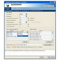
Page 29
... The Finish button is disabled until you correct all the errors indicated in this window. December 2010 Altera Corporation 3. Parameter Settings External Memory Interface Handbook Volume 3 Section II. DDR3 SDRAM Controller with ALTMEMPHY IP User Guide (Figure 3–1) ...
Page 30
... Enable Half Rate Bridge option. 1 When targeting a HardCopy device migration with performance improvement, the ALTMEMPHY IP should target the mid speed grade to ensure that the PLL and the PHY sequencer settings match. The compilation of the design can be executed in the faster speed grade. ...
Page 31
... If you save the new settings in a directory other than the default directory, click Load Preset in the Memory Settings tab to load the settings into the Memory Presets list. December 2010 Altera Corporation Description External Memory Interface Handbook Volume 3 Section II. DDR3 SDRAM Controller with ALTMEMPHY IP User Guide 3–3 ...
Page 32
... FPGA. The percentage values are estimated by Altera based on the process variation. External Memory Interface Handbook Volume 3 Section II. DDR3 SDRAM Controller with ALTMEMPHY IP User Guide Chapter 3: Parameter Settings ALTMEMPHY Parameter Settings December 2010 Altera Corporation ...
Page 33
... JEDEC specification as address mirroring. — — Enter ranks with mirrored addresses in this field. There is one bit per chip select. For example, for four chip selects, enter 1011 to mirror the address on chip select #3, #1, and #0. Register Control Word values for the DDR3 registered — ...
Page 34
... Defines the number of bank address bits for your 3 bits interface. Defines the number of chip selects on each DIMM in your interface. Currently, calibration is done with all ranks but bits you can only perform timing analysis with one single-rank DIMM ...
Page 35
... This option is not supported by the DDR3 SDRAM Controller with ALTMEMPHY IP, so set to Full Array if you are using the Altera controller. 111}, Section II. DDR3 SDRAM Controller with ALTMEMPHY IP User Guide 3–7 Description External Memory Interface Handbook Volume 3 ...
Page 36
... Sets the auto self-refresh method for the memory device. The DDR3 SDRAM Controller with ALTMEMPHY — IP currently does not support the ASR option that you need for extended temperature memory self-refresh. Determines the temperature range for self refresh. You need to also use the optional auto self refresh option — ...
Page 37
... V IL and Hold Timing” on page 3–10 about how to derate this specification. ps The maximum data hold skew factor output hold time. CK Section II. DDR3 SDRAM Controller with ALTMEMPHY IP User Guide Description (dc), not V (dc) min or V (dc) REF IH IL “Derating Memory Setup and Hold ...
Page 38
... See the memory device data sheet for the parameter range. Some of the parameters may be listed in a clock cycle (t Plug-In Manager requires you to enter the value in a time unit (ps or ns), convert the number by multiplying it with the clock period of your interface (and not the maximum clock period listed in the memory data sheet). ...
Page 39
... The calibration of the resynchronization clock on the read side depends on the phase of the memory clock on the write side. Section II. DDR3 SDRAM Controller with ALTMEMPHY IP User Guide 3–11 )/slew_rate = 175 = REF )/slew_rate = 100 + 0 + 100 = ...
Page 40
... All supported device simulation options families External Memory Interface Handbook Volume 3 Section II. DDR3 SDRAM Controller with ALTMEMPHY IP User Guide Description Use this option with Stratix III, Stratix IV, HardCopy III, or HardCopy IV devices, if you want to apply a non-standard phase shift to the DQS capture clock. The ALTMEMPHY DLL offsetting I/O can then be connected to the external DLL and the Offset Control Block ...
Page 41
... CK signals, and the negative values represent the address and command signals that are shorter than the CK signals. (Figure 3–3) allows you to parameterize the following settings: Section II. DDR3 SDRAM Controller with ALTMEMPHY IP User Guide 3–13 Table 3–7. The Description ...
Page 42
... Figure 3–3. DDR3 SDRAM Controller with ALTMEMPHY Settings Controller Settings Table 3–8 shows the options provided on the Controller Settings tab. External Memory Interface Handbook Volume 3 Section II. DDR3 SDRAM Controller with ALTMEMPHY IP User Guide DDR3 SDRAM Controller with ALTMEMPHY Parameter Settings Settings, PHY Settings, and ...
Page 43
... Allows you to control the mapping between the address bits on the Avalon interface and the chip, row, bank, and column bits on the memory interface. If your application issues bursts that are greater than the column size of the memory device, choose the Chip-Row-Bank-Column option ...
Page 44
... Turn on to enable the multi-cast write control on the controller top level. Asserting the multi-cast write control when requesting a write burst causes the write data to be written to all the chip selects in the memory system. When you turn on this option together with the Enable User Auto-Refresh Controls option, HPC II the user refresh commands are issued to all chips ...
Page 45
... Specifies the local side interface between the user logic and the memory controller. The Avalon-MM interface allows you to HPC easily connect to other Avalon-MM peripherals. The HPC II architecture supports only the Avalon-MM interface. Section II. DDR3 SDRAM Controller with ALTMEMPHY IP User Guide 3–17 Description External Memory Interface Handbook Volume 3 ...
Page 46
... External Memory Interface Handbook Volume 3 Section II. DDR3 SDRAM Controller with ALTMEMPHY IP User Guide Chapter 3: Parameter Settings DDR3 SDRAM Controller with ALTMEMPHY Parameter Settings December 2010 Altera Corporation ...
Page 47
... December 2010 Altera Corporation 4. Compiling and Simulating Example Top-Level File ALTMEMPHY High- DLL (1) Performance Controller PLL External Memory Interface Handbook Volume 3 Section II. DDR3 SDRAM Controller with ALTMEMPHY IP User Guide Example Pass or Fail Driver ...
Page 48
... If your design contains pin names that do not match the design, edit the ■ <variation name>_pin_assignments.tcl file before you run the script. To edit the .tcl file, perform the following steps: a. Open <variation name>_pin_assignments.tcl file. b. Based on the flow you are using, set the sopc_mode value to Yes or No. ...
Page 49
... Device & Pin Options dialog box. If you are using any other device and not using advanced I/O timing, specify the output pin loading for all memory interface pins. December 2010 Altera Corporation External Memory Interface Handbook Volume 3 Section II. DDR3 SDRAM Controller with ALTMEMPHY IP User Guide 4–3 ...
Page 50
... External Memory Interface Handbook Volume 3 Section II. DDR3 SDRAM Controller with ALTMEMPHY IP User Guide Tcl scripts and macros that you can use to compile the testbench 351: Simulating Nios II Embedded Processor Chapter 4: Compiling and Simulating Simulating the Design “ ...
Page 51
... Chapter 4: Compiling and Simulating Simulating the Design Full calibration—across all pins and chip selects. This option allows for longer ■ simulation time. Available for ×4 and ×8 DDR3 SDRAM between 300 MHz and 533 MHz. You cannot use the wizard-generated memory model, if you select Full Calibration. ...
Page 52
... External Memory Interface Handbook Volume 3 Section II. DDR3 SDRAM Controller with ALTMEMPHY IP User Guide Chapter 4: Compiling and Simulating Simulating the Design December 2010 Altera Corporation ...
Page 53
... The ALTMEMPHY megafunction creates the datapath between the memory device and the memory controller, and user logic in various Altera devices. The ALTMEMPHY megafunction GUI helps you configure multiple variations of a memory interface. You can then connect the ALTMEMPHY megafunction variation with either a user-designed controller or with an Altera high-performance controller. ...
Page 54
... Clock and reset management, including DLL and PLL ■ Sequencer for calibration ■ Read datapath External Memory Interface Handbook Volume 3 Section II. DDR3 SDRAM Controller with ALTMEMPHY IP User Guide Chapter 5: Functional Description—ALTMEMPHY shows the major blocks of the ALTMEMPHY megafunction FPGA ALTMEMPHY Write ...
Page 55
... Prepare for User Mode” f For more detailed information about each calibration step, refer to the section in volume 4 of the External Memory Interface Handbook. December 2010 Altera Corporation External Memory Interface Handbook Volume 3 Section II. DDR3 SDRAM Controller with ALTMEMPHY IP User Guide 5–3 Debugging ...
Page 56
... All 1: ‘b1111 - DDIO high and low bits held at 1 ■ Toggle: ‘b0101 - DDIO high bits held at 0 and DDIO low bits held at 1 External Memory Interface Handbook Volume 3 Section II. DDR3 SDRAM Controller with ALTMEMPHY IP User Guide Chapter 5: Functional Description—ALTMEMPHY Memory Device and PHY Initialization ...
Page 57
... December 2010 Altera Corporation (“Step 3: Read Resynchronization (Capture) Clock to “Step 4: Read and Write Datapath Section II. DDR3 SDRAM Controller with ALTMEMPHY IP User Guide 5–5 Phase”) are required Timing”) to External Memory Interface Handbook Volume 3 ...
Page 58
... ALTMEMPHY megafunction. The assumption made about the mimic path is that the VT variation on the round trip delay path that resides outside of the FPGA is accounted for in the board skew and memory parameters entered in the MegaWizard Plug-In Manager. For the write direction, any VT variation in the memory devices is accounted for by timing analysis. Figure 5– ...
Page 59
... The DDR3 SDRAM leveling sequencer during calibration writes to the following locations: December 2010 Altera Corporation datain ddiodatain outclk mimic_data_in alt_mem_phy_mimic measure_clk 5–4. DQS/DQ DQS/DQ DQS/DQ CK/CK# DQS/DQ Section II. DDR3 SDRAM Controller with ALTMEMPHY IP User Guide 5– mem_clk_2x ALTPLL measure_clk DQS/DQ DQS/DQ External Memory Interface Handbook Volume 3 ...
Page 60
... The calibration assumes that the skew for all the DQS launch times is one clock period maximum. The VT tracking portion of the DDR3 SDRAM sequencer is similar to that of the DDR or DDR2 SDRAM sequencer. External Memory Interface Handbook Volume 3 Section II. DDR3 SDRAM Controller with ALTMEMPHY IP User Guide Chapter 5: Functional Description—ALTMEMPHY Block Description December 2010 Altera Corporation ...
Page 61
... Read and Write Datapath Timing Address and Command Clock Cycle Postamble Write Clock Path Setup Prepare for User Mode VT Tracking User Mode “Step 8: Prepare for User External Memory Interface Handbook Volume 3 Section II. DDR3 SDRAM Controller with ALTMEMPHY IP User Guide 5–9 Mode”. ...
Page 62
... This step aligns the DQS edge with the CK edge at each memory device in the DIMM, which includes calibrating the write-leveling delay chains, programmable output delay chain, and using the t relationship between the DQS edge and the CK edge. The calibration uses one DQ pin per DQS group (prime DQ) for write leveling calibration. Step 3: Write Training Patterns This step only allows you to write a pattern to be read later to calibrate the read path ...
Page 63
... December 2010 Altera Corporation 5–5. 5–6. Figure 5–6). This applies to all address and command signals in to see the frequency relationship of mem_clk_2x with Section II. DDR3 SDRAM Controller with ALTMEMPHY IP User Guide 5–11 “VT “Mimic External Memory Interface Handbook Volume 3 ...
Page 64
... Figure 5–6 shows a 1T chip select signal (mem_cs_n), which is active low, and disables the command in the memory device. All commands are masked when the chip-select signal is inactive. The mem_cs_n signal is considered part of the command code. Figure 5–6. Arria II GX Address and Command Datapath ...
Page 65
... The Stratix III address and command clock, ac_clk_1x, is half rate. The command and address pins use the DDIO output circuitry to launch commands from either the rising or falling edges of the clock. The chip select (mem_cs_n), clock enable (mem_cke), and mem_odt pins are enabled on one memory clock cycle basis and can be launched ...
Page 66
... Clock Name (1) Counter phy_clk_1x and C0 aux_half_rate_clk mem_clk_2x and C1 aux_full_rate_clk C2 mem_clk_1x C3 write_clk_2x External Memory Interface Handbook Volume 3 Section II. DDR3 SDRAM Controller with ALTMEMPHY IP User Guide Phase Clock Clock Rate (Degrees) Network Type 0° Half-Rate Global 0° Full-Rate Global 0° Half-Rate Global –90° ...
Page 67
... Full-Rate Global Calibrated Full-Rate Global Calibrated Full-Rate Global Section II. DDR3 SDRAM Controller with ALTMEMPHY IP User Guide 5–15 Notes Address and command clock. The ac_clk_2x clock is derived from either mem_clk_2x (when you choose 0° or 180° phase shift) or write_clk_2x (when you choose 90° or 270° phase shift). ...
Page 68
... Clock Name (1) Counter phy_clk_1x and C0 aux_half_rate_clk C1 mem_clk_2x C2 aux_full_rate_clk C3 write_clk_2x C4 resync_clk_2x C5 measure_clk_1x External Memory Interface Handbook Volume 3 Section II. DDR3 SDRAM Controller with ALTMEMPHY IP User Guide Clock Phase Clock Network (Degrees) Rate Type –40° (with leveling) Half-Rate Global 30° (without leveling) 0 Full-Rate Special 0° ...
Page 69
... Q CLR Circuit SET SET reset_n scan_clk pll_ reprogram_ Q Q CLR CLR request pll_reconfig_reset_n pll_reset Section II. DDR3 SDRAM Controller with ALTMEMPHY IP User Guide Notes Address and command clock. SET SET CLR CLR pll_reconfig_ reset_ ams_n_r pll_new_dir pll_locked reset_master_ams phasestep locked phaseupdown ...
Page 70
... DQS input signals at the end of the read postamble time do not cause erroneous data to be captured as a result of postamble glitches. External Memory Interface Handbook Volume 3 Section II. DDR3 SDRAM Controller with ALTMEMPHY IP User Guide phy_clk clk divider ...
Page 71
... Demultiplexing is achieved using a dual-port memory with a 2n-bit wide write-port operating on the resynchronization clock (SDR) and a 4n-bit wide read-port operating on the PHY clock (HDR). The basic principle of operation is that data is written to the memory at the SDR rate and read from the memory at the HDR rate while incrementing the read- and write-address pointers ...
Page 72
... DQS input signals at the end of the read postamble time do not cause erroneous data to be captured as a result of postamble glitches. External Memory Interface Handbook Volume 3 Section II. DDR3 SDRAM Controller with ALTMEMPHY IP User Guide Chapter 5: Functional Description—ALTMEMPHY Block Description December 2010 Altera Corporation ...
Page 73
... December 2010 Altera Corporation Read Datapath dio_rdata3_1x dio_rdata2_1x Dual Port RAM 4n bits wr_data rd_data dio_rdata1_1x wr_clk rd_clk dio_rdata0_1x resync_clk_1x External Memory Interface Handbook Volume 3 Section II. DDR3 SDRAM Controller with ALTMEMPHY IP User Guide 5–21 ram_rdata_1x[4n] Data ctl_rdata[4n] Mapping Logic phy_clk_1x ...
Page 74
... The write data is clocked by the system clock phy_clk_1x at half-data rate (HDR) and reordered into HDR of width four with n-bits each, represented in wdp_wdata0_1x. External Memory Interface Handbook Volume 3 Section II. DDR3 SDRAM Controller with ALTMEMPHY IP User Guide Write Datapath wdp_wdata_h Data Multiplexing ...
Page 75
... December 2010 Altera Corporation Data Ordering wdp_wdata3_1x wdp_wdata2_1x Data wdp_wdata1_1x Ordering wdp_wdata0_1x write_clk_2x phy_clk_1x ctl_clk ctl_wdata Table 5–5 show the signals. Section II. DDR3 SDRAM Controller with ALTMEMPHY IP User Guide ctl_wdata[4n] phy_clk_1x [ Figure 5–13 shows External Memory Interface Handbook Volume 3 5–23 ...
Page 76
... Output mem_we_n (4) Output mem_ac_parity parity_error_n (4) Output External Memory Interface Handbook Volume 3 Section II. DDR3 SDRAM Controller with ALTMEMPHY IP User Guide (Note 1) Width (2) The memory row and column address bus. MEM_IF_ROWADDR_WIDTH The memory bank address bus. MEM_IF_BANKADDR_WIDTH 1 The memory column address strobe. ...
Page 77
... In full-rate designs, a copy of the mem_clk_2x 1 signal that you can use in other parts of your design. Section II. DDR3 SDRAM Controller with ALTMEMPHY IP User Guide 5–25 Description Description External Memory Interface Handbook Volume 3 ...
Page 78
... Read Data Interface Input ctl_doing_rd Output ctl_rdata External Memory Interface Handbook Volume 3 Section II. DDR3 SDRAM Controller with ALTMEMPHY IP User Guide Chapter 5: Functional Description—ALTMEMPHY Width (1) Low frequency scan clock supplied primarily to 1 clock any user logic that interfaces to the PLL and DLL reconfiguration interfaces ...
Page 79
... Allows sharing DLL in this ALTMEMPHY instance with another DQS_DELA ALTMEMPHY instance. Connect the dqs_delay_ctrl_export port Y_CTL_WI on the ALTMEMPHY instance with a DLL to the DTH dqs_delay_ctrl_import port on the other ALTMEMPHY instance. Section II. DDR3 SDRAM Controller with ALTMEMPHY IP User Guide 5–27 Description Description External Memory Interface Handbook Volume 3 ...
Page 80
... Output pll_phase_done I/O Delay Chain Signals—Stratix III, HardCopy III, and HardCopy IV Devices External Memory Interface Handbook Volume 3 Section II. DDR3 SDRAM Controller with ALTMEMPHY IP User Guide Width Allows the use of DLL in another ALTMEMPHY instance in this DQS_DELA ALTMEMPHY instance. Connect the dqs_delay_ctrl_export port ...
Page 81
... The final centre of data valid window size (rsu_codvw_size) is the number of phases where data was successfully read in the — calculation of the resynchronization clock centre of data valid window phase (rsu_codvw_phase). Section II. DDR3 SDRAM Controller with ALTMEMPHY IP User Guide 5–29 Description External Memory Interface Handbook Volume 3 ...
Page 82
... MEM_IF_DQS_WIDTH The row address width of the memory device. MEM_IF_ROWADDR_WIDTH The bank address with the memory device. MEM_IF_BANKADDR_WIDTH The number of chip select pins in the interface. The sequencer only calibrates one chip MEM_IF_CS_WIDTH select pin. The number of mem_dm pins on the memory interface. MEM_IF_DM_WIDTH The number of mem_dq[] pins per mem_dqs pin ...
Page 83
... DIMM for better debugging mechanism. December 2010 Altera Corporation Figure 5–14 shows an overview of the connections AFI PHY ctl_addr ctl_cas_n ctl_we_n Admin Sequencer ctl_rdata Section II. DDR3 SDRAM Controller with ALTMEMPHY IP User Guide 5–31 DDR3 SDRAM mem_dqs mem_dq External Memory Interface Handbook Volume 3 ...
Page 84
... Therefore, for each x16 device, at least two ctl_doing_rd bits need to be driven, and two ctl_rdata_valid bits need to be interpreted. The AFI has the following conventions: External Memory Interface Handbook Volume 3 Section II. DDR3 SDRAM Controller with ALTMEMPHY IP User Guide Chapter 5: Functional Description—ALTMEMPHY and Figure 5–16 display the half-rate write operation ...
Page 85
... Chapter 5: Functional Description—ALTMEMPHY PHY-to-Controller Interfaces With the AFI, high and low signals are combined in one signal, so for a single chip ■ select (ctl_cs_n) interface, ctl_cs_n[1:0], where location 0 appears on the memory bus on one mem_clk cycle and location 1 on the next mem_clk cycle. ...
Page 86
... In all waveforms a command record is added that combines the memory pins ras_n, cas_n and we_n into the current command that is issued. This command is registered by the memory when chip select (mem_cs_n) is low. The important commands in the presented waveforms are WR = write, ACT = activate. ...
Page 87
... Figure 5–18: (1) For AFI, ctl_doing_rd is required to be asserted one memory clock cycle before chip select (ctl_cs_n) is asserted. In the half-rate ctl_clk domain, this requirement manifests as the controller driving 11 (as opposed to the 01) on ctl_doing_rd. (2) AFI requires that ctl_doing_rd is driven for the duration of the read. In this example driven to 11 for two half-rate ctl_clks, which equates to driving to 1, for the four memory clock cycles of this four-beat burst ...
Page 88
... These upper bits can be driven to any value in this alignment. External Memory Interface Handbook Volume 3 Section II. DDR3 SDRAM Controller with ALTMEMPHY IP User Guide Figure 5–20 show spaced word-unaligned writes and reads. ...
Page 89
... Figure 5–20: (1) Similar to word-aligned reads, ctl_doing_rd is asserted one memory clock cycle before chip select (ctl_cs_n) is asserted, which for a word-unaligned read is in the previous controller clock (ctl_clk) cycle. In this example the ctl_doing_rd signal is now spread over three controller clock (ctl_clk) cycles, the high bits in the sequence '10','11','01','10','11','01' providing the required four memory clock cycles of assertion for ctl_doing_rd for the two 4-beat reads in the full-rate memory clock domain, '011110','011110' ...
Page 90
... This signal is synchronously de-asserted with respect to the ctl_clk or phy_clk clock domain and it can reset any additional user logic on that clock domain. External Memory Interface Handbook Volume 3 Section II. DDR3 SDRAM Controller with ALTMEMPHY IP User Guide Chapter 5: Functional Description—ALTMEMPHY 4–1. Using a Custom Controller “ ...
Page 91
... Address and command signals are automatically sized for 1T operation, such that for full-rate designs there is one input bit per pin (for example, one cs_n input per chip select configured); for half-rate designs there are two. If you require a more conservative 2T address and command scheme, use a full-rate design and drive the address/command inputs for two clock cycles half-rate design drive both address/command bits for a given pin identically ...
Page 92
... Board layout ■ Address and command path latency and 1T register setting, which is dynamically setup to take into account any leveling effects External Memory Interface Handbook Volume 3 Section II. DDR3 SDRAM Controller with ALTMEMPHY IP User Guide Chapter 5: Functional Description—ALTMEMPHY Figure 5–22 show these relationships. 1 ...
Page 93
... DDR3 SDRAM on Arria II GX devices make it only possible to use the ctl_dqs_burst signal for the DQS enable in Stratix III devices. December 2010 Altera Corporation Figure 5–23 shows the operation of ctl_wlat port. ctl_wlat = AdAd AdAd External Memory Interface Handbook Volume 3 Section II. DDR3 SDRAM Controller with ALTMEMPHY IP User Guide 5–41 ...
Page 94
... External Memory Interface Handbook Volume 3 Section II. DDR3 SDRAM Controller with ALTMEMPHY IP User Guide Chapter 5: Functional Description—ALTMEMPHY Using a Custom Controller December 2010 Altera Corporation ...
Page 95
... DDR3 SDRAM HPC. DDR3 SDRAM High- Performance Controller Control ALTMEMPHY Logic Megafunction (Encrypted) External Memory Interface Handbook Volume 3 Section II. DDR3 SDRAM Controller with ALTMEMPHY IP User Guide mem_a mem_ba mem_cas_n mem_cke mem_clk mem_clk_n mem_cs_n mem_dm mem_dq ...
Page 96
... This FIFO buffer is sized to be deeper than the command FIFO buffer to prevent it from filling up and interrupting streaming writes. External Memory Interface Handbook Volume 3 Section II. DDR3 SDRAM Controller with ALTMEMPHY IP User Guide Chapter 6: Functional Description—High-Performance Controller Timer Logic Initialization ...
Page 97
... When the state machine wants to issue a command to the memory, it asserts a set of internal signals. The address and command decode logic turns these into the DDR-specific RAS, CAS, and WE commands. December 2010 Altera Corporation RCD External Memory Interface Handbook Volume 3 Section II. DDR3 SDRAM Controller with ALTMEMPHY IP User Guide 6–3 ). The timer ...
Page 98
... PHY Interface Logic When the main state machine issues a write command to the memory, the write data for that write burst has to be fetched from the write data FIFO buffer. The relationship between write command and write data depends on the memory type, ALTMEMPHY interface type, CAS latency, and the full-rate or half-rate setting ...
Page 99
... NOP High High ACT Low High RD High Low WR High Low PCH Low High ARF Low Low LMR Low Low External Memory Interface Handbook Volume 3 Section II. DDR3 SDRAM Controller with ALTMEMPHY IP User Guide 6–5 we_n High High High Low Low High Low ...
Page 100
... The encoder—encodes the 64-bit message to a 72-bit codeword ■ The decoder-corrector—decodes and corrects the 72-bit codeword if possible ■ External Memory Interface Handbook Volume 3 Section II. DDR3 SDRAM Controller with ALTMEMPHY IP User Guide Chapter 6: Functional Description—High-Performance Controller ECC Write Write ...
Page 101
... Detected and/or corrected single-bit errors ■ Detected double-bit errors ■ The ECC logic can instantiate multiple encoders, each running in parallel, to encode any width of data words assuming they are integer multiples of 64. The ECC logic operates between the local (native or Avalon-MM interface) and the memory controller. ...
Page 102
... Avalon-MM interface. The new write word is written to the memory location. A separate field in the interrupt status register highlights this condition. External Memory Interface Handbook Volume 3 Section II. DDR3 SDRAM Controller with ALTMEMPHY IP User Guide Chapter 6: Functional Description—High-Performance Controller December 2010 Altera Corporation ...
Page 103
... A partial write results in a read followed by write in the ECC logic, so latency depends on the time the controller takes to fetch the data from the particular address. December 2010 Altera Corporation 89ABCDEF 01234567 01234567 Section II. DDR3 SDRAM Controller with ALTMEMPHY IP User Guide External Memory Interface Handbook Volume 3 ...
Page 104
... Current single-bit error 03 count Current double-bit error 04 count Last or first single-bit error 05 error address External Memory Interface Handbook Volume 3 Section II. DDR3 SDRAM Controller with ALTMEMPHY IP User Guide Chapter 6: Functional Description—High-Performance Controller Rate 1 Half 2 Full Size Attribute Default (Bits) ...
Page 105
... RO 00000000 These status bits can be cleared by writing the respective locations. This register stores the interrupt mask 00000001 four fields (refer to Section II. DDR3 SDRAM Controller with ALTMEMPHY IP User Guide 6–11 Description Table 6–6). Table 6–7). External Memory Interface Handbook Volume 3 ...
Page 106
... ECC corruption type 10 First or last error 11 Clear interrupt External Memory Interface Handbook Volume 3 Section II. DDR3 SDRAM Controller with ALTMEMPHY IP User Guide Chapter 6: Functional Description—High-Performance Controller Size Attribute Default (Bits) This status register stores the occurrence of single-bit error for each 64-bit part of ...
Page 107
... When 0, interrupt when double-bit error occurs during a read-modify-write condition (partial write). Reserved Reserved. Name When 0, no single-bit error; when 1, single-bit Interrupt error occurred in this 64-bit part. Reserved Reserved. Section II. DDR3 SDRAM Controller with ALTMEMPHY IP User Guide 6–13 Description Description Description External Memory Interface Handbook Volume 3 ...
Page 108
... External Memory Interface Handbook Volume 3 Section II. DDR3 SDRAM Controller with ALTMEMPHY IP User Guide Chapter 6: Functional Description—High-Performance Controller Bit Name Cause of Interrupt Reserved DDR3 SDRAM Controller ...
Page 109
... The addresses are then read back to ensure that the controller has issued the correct signals to the memory. This test is only applicable when the local burst size is two. You can skip this test by setting the test_incomplete_writes_on signal to logic zero. ...
Page 110
... The example driver generates a series of write and read requests starting with an all-zeros pattern, a walking-one pattern, a walking-zero pattern, and ending with an all-zeros pattern. This test checks to make sure that all the individual address bits are operating correctly. You can skip this test by setting the test_addr_pin_on signal to logic zero. ■ ...
Page 111
... For multiple chip selects: width = chip bits + bank bits + row bits + column bits – the bank address is 3 bits wide, row is 14 bits wide and column is 10 bits wide, then the local address is 25 bits wide. To map local_address to bank, ...
Page 112
... Input local_autopch_req External Memory Interface Handbook Volume 3 Section II. DDR3 SDRAM Controller with ALTMEMPHY IP User Guide Chapter 6: Functional Description—High-Performance Controller Description Avalon burst begin strobe, which indicates the beginning of an Avalon burst. This signal is only available when the local interface is an Avalon-MM interface and the memory burst length is greater than 2 ...
Page 113
... Read data bus. The width of local_rdata is four times the memory data bus. Asserted if the current read data has an error. This signal is only available if the Enable error detection and correction logic is turned on. Section II. DDR3 SDRAM Controller with ALTMEMPHY IP User Guide 6–19 External Memory Interface Handbook Volume 3 ...
Page 114
... The mem_clk signals are output only signals from the FPGA. However, in the Quartus II software they must be defined as bidirectional (INOUT) I/Os to support the mimic path structure that the ALTMEMPHY megafunction uses. External Memory Interface Handbook Volume 3 Section II. DDR3 SDRAM Controller with ALTMEMPHY IP User Guide Chapter 6: Functional Description—High-Performance Controller Description Read data valid signal ...
Page 115
... Read request for ECC logic. Input ECC logic write data. Input Write request for ECC logic. Output Interrupt from ECC logic. Output Return data from ECC logic. External Memory Interface Handbook Volume 3 Section II. DDR3 SDRAM Controller with ALTMEMPHY IP User Guide 6–21 ...
Page 116
... External Memory Interface Handbook Volume 3 Section II. DDR3 SDRAM Controller with ALTMEMPHY IP User Guide Chapter 6: Functional Description—High-Performance Controller Top-level Signals Description December 2010 Altera Corporation ...
Page 117
... HPC II replaces the port interface level for the AFI and Avalon interface without requiring any top-level change. December 2010 Altera Corporation 7. Functional Description— High-Performance Controller II =40 ns, t =10 ns, t FAW RRD External Memory Interface Handbook Volume 3 Section II. DDR3 SDRAM Controller with ALTMEMPHY IP User Guide =10 ns. RTP ...
Page 118
... The side-band signals differ slightly for HPC II. If you use these signals, you need ■ to perform the following steps. ■ local_refresh_req You need to drive an additional active high signal, local_refresh_chip, to control which chip to issue the user-refresh to. ■ local_powerdn_req The user-manual power signal is no longer supported in HPC II. Instead, you ...
Page 119
... The Avalon-MM data slave interface accepts read and write requests from the Avalon-MM master. The width of the data, local_wdata and local_rdata, is four times the width of the external memory. The local address width is sized based on the memory chip, row, bank, and column address widths. For example: ■ ...
Page 120
... Bank Management Logic The bank management logic keeps track of the current state in each bank across multiple chips. It can keep a row open in every bank in your memory system. When a command is issued by the state machine, the bank management logic is updated with the latest bank status. The main state machine uses its look-ahead capability to issue early bank management commands ...
Page 121
... The write and read datapath, and the write data timing logic generate the AFI read and write control signals. When the state machine issues a write command to the memory, the IP core gets the write data for that write burst from the write data FIFO buffer. The relationship between the write command and write data depends on the afi_wlat signal ...
Page 122
... Multi-Cast Write The multi-cast write request signal allows you to ask the controller to send the current write requests to all the chip selects. This means that the write data is written to all the ranks in the system. The multi-cast write feature is useful for t you can cycle through chips to continuously read data without hitting t multi-cast write is not supported for registered DIMM interfaces or when the ECC logic is enabled ...
Page 123
... Hamming code ECC logic that encodes every bits of data into bits of codeword. December 2010 Altera Corporation through Table 7–23 in page 7–18 Section II. DDR3 SDRAM Controller with ALTMEMPHY IP User Guide 7–7 for detailed information about the External Memory Interface Handbook Volume 3 ...
Page 124
... For partial writes, the ECC logic performs the following steps: External Memory Interface Handbook Volume 3 Section II. DDR3 SDRAM Controller with ALTMEMPHY IP User Guide Chapter 7: Functional Description—High-Performance Controller II December 2010 Altera Corporation ...
Page 125
... HPC II. Figure 7–4. Partial Burst for HPC II local_address local_size local_be local_wdata mem_dm mem_dq December 2010 Altera Corporation 89ABCDEF 01234567 01234567 Section II. DDR3 SDRAM Controller with ALTMEMPHY IP User Guide External Memory Interface Handbook Volume 3 7–9 ...
Page 126
... The full-array memory model (<variation name>_mem model_full.v) allocates memory for all addresses accessible by the DDR cores. This allocation makes it impossible to simulate large memory designs. External Memory Interface Handbook Volume 3 Section II. DDR3 SDRAM Controller with ALTMEMPHY IP User Guide Chapter 7: Functional Description—High-Performance Controller II DDR SDRAM Controller Generated ...
Page 127
... MAX_ROW, MAX_BANK, and MAX_COL constants in the example driver source code, and the entire memory space can be tested by adjusting these values. You can skip this test by setting the test_seq_addr_on signal to logic zero. Incomplete write operation ■ ...
Page 128
... Table 7–4. Clock and Reset Signals (Part Name global_reset_n pll_ref_clk phy_clk reset_phy_clk_n External Memory Interface Handbook Volume 3 Section II. DDR3 SDRAM Controller with ALTMEMPHY IP User Guide Chapter 7: Functional Description—High-Performance Controller II Test Sequential address test Incomplete write test Data mask pin test Address pin test ...
Page 129
... Allows the use of DLL in another ALTMEMPHY instance in this ALTMEMPHY instance. Connect the export port on the ALTMEMPHY Input instance with a DLL to the import port on the other ALTMEMPHY instance. Section II. DDR3 SDRAM Controller with ALTMEMPHY IP User Guide 7–13 Description External Memory Interface Handbook Volume 3 ...
Page 130
... For multiple chip selects: width = chip bits + row bits + bank bits + column bits – the bank address is 2 bits wide, row is 13 bits wide and column is 10 bits wide, then the local address is 23 bits wide. To map local_address to ...
Page 131
... For example: If the local_refresh_chip signal is assigned with a value of 4’b0101, the controller refreshes the memory chips 0 and 2, and memory chips 1 and 3 are not refreshed. If you turn on the Enable Multi-cast Write Control option, this signal is ignored ...
Page 132
... Output csr_rdata[] External Memory Interface Handbook Volume 3 Section II. DDR3 SDRAM Controller with ALTMEMPHY IP User Guide Chapter 7: Functional Description—High-Performance Controller II Description Read data bus. The width of local_rdata is twice that of the memory data bus for a full rate controller; four times the memory data bus for a half rate controller ...
Page 133
... Active-low signal that is asserted when a parity error occurs and stays asserted until the PHY is reset. Signal sent from the DIMM to the PHY to indicate that a parity error has occured for a particular cycle. Section II. DDR3 SDRAM Controller with ALTMEMPHY IP User Guide 7–17 External Memory Interface Handbook Volume 3 ...
Page 134
... Table 7–9. Register Map Address ALTMEMPHY Register Map Controller Register Map External Memory Interface Handbook Volume 3 Section II. DDR3 SDRAM Controller with ALTMEMPHY IP User Guide Chapter 7: Functional Description—High-Performance Controller II Debug interface clock Debug interface address Debug interface chip select Debug interface write request ...
Page 135
... MegaWizard Additive Latency — RW setting for your controller instance. You must set this value in CSR interface register map 0x126 (Table Section II. DDR3 SDRAM Controller with ALTMEMPHY IP User Guide using the Avalon-MM protocol. (Table 7–12) for the mode register “DDR3 SDRAM With Description (Table 7– ...
Page 136
... RTT_WR 15:11 Reserved 17:16 MPR_RF 18 MPR 31:19 Reserved External Memory Interface Handbook Volume 3 Section II. DDR3 SDRAM Controller with ALTMEMPHY IP User Guide Chapter 7: Functional Description—High-Performance Controller II Access Not used by the controller, but you can set and 0 RW program into the memory device mode register. ...
Page 137
... This bit indicates that the memory power-down state. Section II. DDR3 SDRAM Controller with ALTMEMPHY IP User Guide 7–21 Table 7–6 using Description You must not use this register during the ALTMEMPHY megafunction calibration ...
Page 138
... ADDR_ORDER 22 REGDIMM 24:23 CTRL_DRATE 30:24 Reserved External Memory Interface Handbook Volume 3 Section II. DDR3 SDRAM Controller with ALTMEMPHY IP User Guide Chapter 7: Functional Description—High-Performance Controller II Default Access Setting this bit, or asserting the 0 RW local_self_rfsh signal, causes the memory to go into self-refresh state. ...
Page 139
... DQ pins per DQS pin (typically 8). Default Access The number of chip select in binary representation. — RW For example, a design with 2 chip selects has the value of 00000011. 0 — Reserved for future use. Section II. DDR3 SDRAM Controller with ALTMEMPHY IP User Guide 7–23 Description ...
Page 140
... REFI 23:16 t RFC 31:24 Reserved External Memory Interface Handbook Volume 3 Section II. DDR3 SDRAM Controller with ALTMEMPHY IP User Guide Chapter 7: Functional Description—High-Performance Controller II Default Access The activate to read or write a timing parameter. — RW The range of legal values is 2-11 cycles. The activate to activate a timing parameter. The — ...
Page 141
... Set to 1 when any single-bit errors occur Set to 1 when any double-bit errors occur. 0 — Reserved for future use. Section II. DDR3 SDRAM Controller with ALTMEMPHY IP User Guide Description ). You must set this WR Description When 1, enables the generation and checking of ECC. When 1, enables auto-correction when a single-bit error is detected ...
Page 142
... Reserved Table 7–23. Address 0x132 ECC Error Address Register Bit Name 31:0 ERR_ADDR External Memory Interface Handbook Volume 3 Section II. DDR3 SDRAM Controller with ALTMEMPHY IP User Guide Chapter 7: Functional Description—High-Performance Controller II Default Access Reports the number of single-bit errors that have 0 RO occurred since the status register counters were last cleared ...
Page 143
... No refresh cycles occur before the transaction. The latency for the high-performance controller comprises many different stages of the memory interface. December 2010 Altera Corporation 8. Latency External Memory Interface Handbook Volume 3 Section II. DDR3 SDRAM Controller with ALTMEMPHY IP User Guide ...
Page 144
... CAS latency (T3) + PHY read data input latency (T4) Similarly, the write latency in the high-performance controllers is made up of three components: write latency = controller latency (T1) + write data latency (T2+T3) External Memory Interface Handbook Volume 3 Section II. DDR3 SDRAM Controller with ALTMEMPHY IP User Guide PHY Latency T2 Address/Command Generation Core ...
Page 145
... Rate (MHz) Type Read Half 400 Write Read Half 400 Write chapter of the Stratix III Device Handbook and the chapter of the Stratix IV Device Section II. DDR3 SDRAM Controller with ALTMEMPHY IP User Guide 8–3 Total Latency Local Clock Time Cycles (ns) 23 115 115 ...
Page 146
... External Memory Interface Handbook Volume 3 Section II. DDR3 SDRAM Controller with ALTMEMPHY IP User Guide Chapter 8: Latency December 2010 Altera Corporation ...
Page 147
... Write for Avalon Interface” ■ “Half Rate Write for Native Interface” ■ “Initialization Timing for HPC” “Calibration Timing for HPC” ■ December 2010 Altera Corporation 9. Timing Diagrams External Memory Interface Handbook Volume 3 Section II. DDR3 SDRAM Controller with ALTMEMPHY IP User Guide ...
Page 148
... The auto-precharge request goes high. (2) The local_ready signal is asserted and remains high until the auto-precharge request goes low. (3) A new row address begins. External Memory Interface Handbook Volume 3 Section II. DDR3 SDRAM Controller with ALTMEMPHY IP User Guide 004 008 00C 010 ...
Page 149
... The local refresh request signal is asserted. (2) The controller asserts the local_refresh_ack signal. (3) The auto-refresh (ARF) command on the command bus. December 2010 Altera Corporation [1] [2] NOP ARF NOP [3] External Memory Interface Handbook Volume 3 Section II. DDR3 SDRAM Controller with ALTMEMPHY IP User Guide 9–3 ...
Page 150
Half-Rate Read for Avalon Interface Figure 9–3. Half-Rate Read Operation for HPC Using Avalon-MM Interface [1] [2] phy_clk Local Interface local_read_req local_write_req local_row_addr[13:0] 0000 local_col_addr[9:0] 000 000 local_bank_addr[2:0] mem_local_addr[24:0] 0000000 0000200 local_size[1:0] local_burstbegin local_rdata[31:0] local_rdata_valid local_read_req local_ready Controller - AFI ...
Page 151
... These are the data to the controller with the valid signal. 7. The controller returns the valid read data to the user logic by asserting the local_rdata_valid signal when there is valid local read data. December 2010 Altera Corporation Figure External Memory Interface Handbook Volume 3 Section II. DDR3 SDRAM Controller with ALTMEMPHY IP User Guide 9–5 9–3: ...
Page 152
Half-Rate Write for Avalon Interface Figure 9–4. Half-Rate Write Operation for HPC Using Avalon Interface [1] [2] [3] phy_clk Local Interface local_write_req local_read_req local_row_addr[13:0] local_col_addr[9:0] 000 local_bank_addr[2:0] mem_local_addr[24:0] 0000100 local_size[1:0] local_be[3:0] local_wdata[31:0] 0578FF82 5D6B3107 local_write_req local_ready Controller - AFI ddr_a[13:0] ...
Page 153
... The write (WR) command on the command bus. 5. The valid write data on the ctl_wdata signal. 6. The valid data on the mem_dq signal goes to the controller. December 2010 Altera Corporation Figure External Memory Interface Handbook Volume 3 Section II. DDR3 SDRAM Controller with ALTMEMPHY IP User Guide 9–7 9–4: ...
Page 154
Half Rate Write for Native Interface Figure 9–5. Half-Rate Write Operation for HPC Using Native Interface [1] [2] [3] [4] phy_clk Local Interface local_wdata_req local_write_req local_read_req local_row_addr[13:0] 0000 0001 local_col_addr[9:0] 000 local_bank_addr[2:0] 0 mem_local_addr[24:0] 0000000 0400102 local_size[1:0] local_be[3:0] local_wdata[31:0] 230F7B57 ...
Page 155
... The write (WR) command on the command bus. 6. The valid write data on the ctl_wdata signal. 7. The valid data on the mem_dq signal goes to the controller. December 2010 Altera Corporation Figure External Memory Interface Handbook Volume 3 Section II. DDR3 SDRAM Controller with ALTMEMPHY IP User Guide 9–9 9–5: ...
Page 156
Initialization Timing Figure 9–6. Initialization Timing for HPC [1] [2] global_reset_n pll_locked phs_shft_busy seq_pll_select[3:0] seq_pll_start_reconfig seq_pll_inc_dec_n seq_ac_ras_n[1:0] seq_ac_cas_n[1:0] seq_ac_we_n[1:0] memory_0_0.ck memory_0_0.ck_n memory_0_0.cke memory_0_0.cs_n memory_0_0.addr[13:0] memory_0_0.ras_n memory_0_0.cas_n memory_0_0.we_n memory_0_0.odt memory_0_0.ba[2] memory_0_0.ba[1] memory_0_0.ba[0] memory_0_0.rst_n memory_0_0.dq[7:0] memory_0_0.dqs memory_0_0.dqs_n memory_0_0.dm_tdqs memory_0_1.ck memory_0_1.ck_n memory_0_1.cke memory_0_1.cs_n ...
Page 157
... The PHY initialization stage; wait for PLL to unlock. 2. The DRAM initialization stage; reset sequence. 3. Various SDRAM bus commands during the initialization sequence. December 2010 Altera Corporation Figure External Memory Interface Handbook Volume 3 Section II. DDR3 SDRAM Controller with ALTMEMPHY IP User Guide 9–11 9–6: ...
Page 158
Calibration Timing Figure 9–7. Calibration Timing for HPC [1] global_reset_n pll_locked phs_shft_busy seq_pll_select[3:0] seq_pll_start_reconfig seq_pll_inc_dec_n state[1:0] seq_ac_ras_n[1:0] seq_ac_cas_n[1:0] seq_ac_we_n[1:0] scan_enable_dq scan_enable_dqs mem_cas_n mem_ras_n mem_we_n memory_0_1.ba[0] memory_0_0.ck memory_0_0.ck_n 3 333 3333 memory_0_0.cke memory_0_0.cs_n memory_0_0.addr[13:0] memory_0_0.cas_n 1 ...
Page 159
... Read With Gaps” ■ ■ “Half-Rate Write With Gaps” ■ “Half-Rate Write Operation (Merging Writes)” ■ “Write-Read-Write-Read Operation” December 2010 Altera Corporation Figure External Memory Interface Handbook Volume 3 Section II. DDR3 SDRAM Controller with ALTMEMPHY IP User Guide 9–13 9–7: ...
Page 160
Half-Rate Read (Burst-Aligned Address) Figure 9–8. Half-Rate Read Operation for HPC II—Burst-Aligned Address [1] [2] phy_clk Local Interface local_address[25:0] 0000000 0000002 0000004 local_size[4:0] local_ready local_burstbegin local_read_req local_rdata[31:0] local_rdata_valid local_be[3:0] Controller - AFI afi_addr[27:0] afi_ba[5:0] afi_cs_n[3:0] AFI Command[2:0] afi_dm[3:0] afi_dqs_burst[0] afi_dqs_burst[1] ...
Page 161
... ECC logic is disabled, there is no delay between the afi_rdata and the local_rdata buses. If there is ECC logic in the controller, there is one or three clock cycles of delay between the afi_rdata and local_rdata buses. December 2010 Altera Corporation Figure External Memory Interface Handbook Volume 3 Section II. DDR3 SDRAM Controller with ALTMEMPHY IP User Guide 9–15 9–8: ...
Page 162
Half-Rate Write (Burst-Aligned Address) Figure 9–9. Half-Rate Write Operation for HPC II—Burst-Aligned Address [1] phy_clk Local Interface local_address[25:0] local_size[4:0] 02 local_ready local_burstbegin local_be[3:0] local_write_req local_wdata[31:0] Controller - AFI afi_addr[27:0] afi_ba[5:0] afi_cs_n[3:0] AFI Command[2:0] afi_dm[3:0] afi_wlat[4:0] afi_dqs_burst[0] afi_dqs_burst[1] afi_wdata[31:0] afi_wdata_valid[1:0] AFI ...
Page 163
... The user logic asserts a second local_write_req signal with size of 2 and address of 0 (col = 0, row = 0, bank = 0, chip = 0). The local_ready signal is asserted along with the local_write_req signal, which indicates that the controller has accepted this request, and the user logic can request another read or write in the following clock cycle ...
Page 164
Half-Rate Read (Non Burst-Aligned Address) Figure 9–10. Half-Rate Read Operation for HPC II—Non Burst-Aligned Address [1] phy_clk Local Interface local_address[25:0] 00000 00001 00003 00005 local_size[4:0] 2 local_ready local_burstbegin local_read_req local_rdata[31:0] local_rdata_valid local_be[3:0] Controller - AFI afi_addr[27:0] afi_ba[5:0] afi_cs_n[3:0] AFI Command[2:0] ...
Page 165
... ECC logic is disabled, there is no delay between the afi_rdata and the local_rdata buses. If there is ECC logic in the controller, there is one or three clock cycles of delay between the afi_rdata and local_rdata buses. December 2010 Altera Corporation Figure External Memory Interface Handbook Volume 3 Section II. DDR3 SDRAM Controller with ALTMEMPHY IP User Guide 9–19 9–10: ...
Page 166
Half-Rate Write (Non Burst-Aligned Address) Figure 9–11. Half-Rate Write Operation for HPC II—Non Burst-Aligned Address [1] phy_clk Local Interface local_address[25:0] 0000001 0000003 local_size[4:0] 2 local_ready local_burstbegin local_be[3:0] local_write_req local_wdata[31:0] AABBCCDD EEFF0011 AABBCCDD Controller - AFI afi_addr[27:0] afi_ba[5:0] afi_cs_n[3:0] AFI Command[2:0] ...
Page 167
... The controller generates another write because the first write non-aligned memory address, 0×0004. The controller performs the second write burst at the memory address of 0×0008. December 2010 Altera Corporation Figure External Memory Interface Handbook Volume 3 Section II. DDR3 SDRAM Controller with ALTMEMPHY IP User Guide 9–21 9–11: ...
Page 168
Half-Rate Read With Gaps Figure 9–12. Half-Rate Read Operation for HPC II—With Gaps [1] [2] [3] phy_clk Local Interface local_address[25:0] 0000810 0000912 0000A14 local_size[4:0] 2 local_ready local_burstbegin local_read_req local_rdata[31:0] local_rdata_valid local_be[3:0] Controller - AFI afi_addr[27:0] afi_ba[5:0] afi_cs_n[3:0] AFI Command[2:0] afi_dm[3:0] ...
Page 169
... Mem Command[2:0] NOP mem_dqs mem_dm mem_dq[7:0] 00 mem_odt[1:0] December 2010 Altera Corporation [6] 0000F1C 2 EEFF0011 AABBCCDD 40C1030 NOP F EEFF0011 7 1030 WR [2] [5] Section II. DDR3 SDRAM Controller with ALTMEMPHY IP User Guide Figure 9–12 AABBCCDD EEFF0011 3 0 NOP [4] [3] External Memory Interface Handbook Volume 3 9–23 00 ...
Page 170
... AFI Memory Interface mem_cke mem_clk mem_ba[2:0] mem_addr[13:0] mem_cs_n[0] Mem Command[2:0] mem_dqs mem_dm mem_dq[7:0] mem_odt[1:0] External Memory Interface Handbook Volume 3 Section II. DDR3 SDRAM Controller with ALTMEMPHY IP User Guide [2] [3] 0000003 00000000 0000000 4001000 0000000 4021008 ACT NOP WR NOP ...
Page 171
... ALTMEMPHY megafunction issues to the memory. 6. The ALTMEMPHY megafunction issues the write command, and sends the write data and write DQS to the memory. December 2010 Altera Corporation Figure External Memory Interface Handbook Volume 3 Section II. DDR3 SDRAM Controller with ALTMEMPHY IP User Guide 9–25 9–14: ...
Page 172
Write-Read-Write-Read Operation Figure 9–15. Write-Read Sequential Operation for HPC II [1] [2] [3] [4] phy_clk Local Interface local_address[25:0] 0000002 0000004 0000006 local_size[4:0] local_ready local_burstbegin local_read_req local_rdata[31:0] 00000000 00000000 local_rdata_valid local_be[3:0] local_write_req local_wdata[31:0] 00000008 00000010 00000018 Controller - AFI afi_addr[27:0] 0000000 ...
Page 173
... The ALTMEMPHY megafunction returns the first data read to the controller after resynchronizing the data to the phy_clk domain, by asserting the afi_rdata_valid signal when there is valid read data on the afi_rdata bus. December 2010 Altera Corporation Figure External Memory Interface Handbook Volume 3 Section II. DDR3 SDRAM Controller with ALTMEMPHY IP User Guide 9–27 9–15: ...
Page 174
... If there is ECC logic in the controller, there is one or three clock cycles of delay between the afi_rdata and local_rdata buses. External Memory Interface Handbook Volume 3 Section II. DDR3 SDRAM Controller with ALTMEMPHY IP User Guide Chapter 9: Timing Diagrams DDR3 High-Performance Controllers II December 2010 Altera Corporation ...
Page 175
... Added information for new GUI parameters: Controller latency, Enable reduced bank ■ tracking for area optimization, and Number of banks to track. July 2010 2.0 Removed information about IP Advisor. This feature is removed from the DDR3 SDRAM ■ IP support for version 10.0. February 2010 1.3 Corrected typos ...
Page 176
... External Memory Interface Handbook Volume 3 Section II. DDR3 SDRAM Controller with ALTMEMPHY IP User Guide Meaning Indicate command names, dialog box titles, dialog box options, and other GUI labels. For example, Save As dialog box. For GUI elements, capitalization matches the GUI. Indicates directory names, project names, disk drive names, file names, file name extensions, software utility names, and GUI labels ...