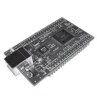
MORPH-IC 1K BLK FTDI, MORPH-IC 1K BLK Datasheet - Page 5

MORPH-IC 1K BLK
Manufacturer Part Number
MORPH-IC 1K BLK
Description
Interface Modules & Development Tools Obsolete See MORPH-IC-II
Manufacturer
FTDI
Datasheet
1.MORPH-IC_1K_BLK.pdf
(9 pages)
Specifications of MORPH-IC 1K BLK
Lead Free Status / RoHS Status
Lead free / RoHS Compliant
Other names
626-DLP-MORPHIC-OEM
Figure 3 shows the programming interface between the FT2232C and the EP1K10TC-100. It uses the
multi-protocol synchronous serial engine feature ( MPSSE ) of the FT2232C channel A to program the
FPGA “on-the-fly”. The FPGA can be programmed / reprogrammed in under 0.2 seconds which makes
it possible to design some type of products that would not normally fit into this size of FPGA by using
several different configuration files for different modes of operation and loading / re-loading these
transparently to the end-user. The configuration files are output from the Altera Quartus ™ software
and can be downloaded into the FPGA either manually by using the loader program supplied or under
application software control by using the DLL supplied.
For further details of MPSSE operation, consult the FT2232C data sheet and the application note
AN2232C-01 downloadable from FTDI’s web site at page http://www.ftdichip.com/FT2232C2.htm. The
source code for the loader program and the DLL illustrate how to program the MPSSE as an Altera
ACEX series loader. MORPH-IC uses the GPIOL0 pin of the FT2232C to detect / verify the completion of
FPGA device configuration and the GPIOL3 pin of the FT2232C to provide a reset to the FPGA via pin
79.
FIGURE 4 - MORPH-IC FPGA DATA TRANSFER INTERFACE
Figure 4 shows the bi-directional data transfer interface between the FT2232C and the EP1K10TC-100.
It uses the FIFO mode of the FT2232C channel B to allow the FPGA to communicate with a PC over
USB. Data is read / written between the devices over an 8 bit data bus BD0 .. BD7.
A typical application would send “commands” to the FPGA which would be interpreted by a state
machine inside the FPGA. Some commands may return data from the FPGA to the application.
To send data to the application poll TXE# until it is low then place the data to be transmitted on BD0 ..
BD7. Enable the bus, strobe the WR pin high then low then disable ( tri-state ) the data bus pins. Data
is written into the FT2232C on the falling edge of WR.
To receive commands / data from the application, poll RXF# until it is low which means that there is
data in the FT2232C to be read. Take RD# low to enable the data from the FT2232C on BD0 .. BD7.
Strobe the data into the FPGA and make RD# high ( its default state ) to tri-state the bus.
For further details of the FT2232C FIFO mode including timings please consult the FT2232C data sheet.
The example project on the CD illustrates such an application. Full VHDL source code of the project and
the Delphi 5 application program are pubished on the CD and are a good starting point for developing
MORPH-IC projects.
Note : The data bus and interface pins are all brought out on the J1 / J2 IO connectors. The data bus
can be used to send / receive data to other external devices when the FT2232C interface is in its idle
state.
MORPH-IC Data Sheet Revision 1.0
MORPH-IC FPGA DATA TRANSFER INTERFACE
USB INTERFACE
FT2232C
I.C.
40
39
38
37
36
35
33
32
30
29
28
27
26
BD4
BD5
BD6
BD7
RD#
RXF#
WR
SI/WUB
BD0
BD1
BD2
BD3
TXE#
FIFO INTERFACE
© Future Technology Devices International Ltd 2004
IO
IO
IO
IO
IO
IO
IO
IO
IO
IO
IO
IO
IO
47
48
49
50
55
56
57
58
61
62
63
64
65
ALTERA ACEX
EP1K10-100
FPGA


