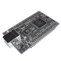
MORPH-IC 1K BLK FTDI, MORPH-IC 1K BLK Datasheet - Page 7

MORPH-IC 1K BLK
Manufacturer Part Number
MORPH-IC 1K BLK
Description
Interface Modules & Development Tools Obsolete See MORPH-IC-II
Manufacturer
FTDI
Datasheet
1.MORPH-IC_1K_BLK.pdf
(9 pages)
Specifications of MORPH-IC 1K BLK
Lead Free Status / RoHS Status
Lead free / RoHS Compliant
Other names
626-DLP-MORPHIC-OEM
TABLE 1 - MORPH-IC IO CONNECTOR PINOUT DESCRIPTION
NOTE 1 - The maximum combined current that can be drawn from these power sources to power
external circuitry is 250mA in total. If a 5V supply is required, use VCC ( 5V ) instead of VCC ( USB ) to
guarantee meeting USB current draw in USB suspend / sleep state ( < 0.5mA ).
Non-Shared IO Pins
Shared IO Pins
Dedicated Input Pins
FT2232C Handshaking
CLKIN
RESETIN#
VCC ( USB )
** Note 1
VCC ( 5V )
** Note 1
VCC ( 3.3V )
** Note 1
GND
N/C
MORPH-IC Data Sheet Revision 1.0
IO6, IO7, IO9, IO13, IO14,
IO15, IO16, IO19, IO20, IO21,
IO22, IO23, IO26, IO27, IO28,
IO30, IO31, IO32, IO33, IO34,
IO43, IO45, IO46, IO68, IO69,
IO70, IO71, IO77, IO78, IO80,
IO81, IO82, IO84, IO85, IO86,
IO94
BD0(IO47), BD1(IO48),
BD2(IO49), BD3(IO50),
BD4(IO55), BD5(IO56),
BD6(IO57), BD7(IO58)
IN38, IN40, IN89, IN91
BC0(RXF#), BC1(TXE#),
BC2(RD#), BC3(WR)
J2-14
J1-14
J1-1
J1-2
J1-17, J1-18, J1-29,
J1-31, J2-17, J2-18,
J2-29, J2-31
J1-11, J1-12, J1-23,
J1-24, J1-35, J1-36,
J2-11, J2-12, J2-23,
J2-24, J2-35, J2-36
J1-37, J2-5, J2-6
MORPH-IC PIN DESCRIPTIONS
© Future Technology Devices International Ltd 2004
These are IO pins from the
EP1K10TC100. The naming convention
is IOxx where xx equals the pin
number of the FPGA. For example,
IO70 is the IO pin on pin 70 of the
device.
These are shared with the FT2232C
data bus and can be used when the
FT2232C data bus is in idle mode.
See above notes on the FT2232C data
transfer interface.
These are input pins from the
EP1K10TC100. The naming convention
is INxx where xx equals the pin number
of the FPGA. For example, IN40 is the
input pin on pin 40 of the device. All
inputs are pulled up to 3.3v by an on-
board 10k resistor.
These would not normally be connected
to external logic, but are brought out
for debug purposes i.e. for connecting
a logic analyzer.
Secondary input clock source from pin
39 of the EP1K10TC100.
Pulling this low resets the FT2232C I.C.
and disconnects the device from the
USB bus. Not normally required but
available if needed. Pulled up to 5v by
an internal 10k resistor.
4.4V to 5.25V un-switched power from
USB with J1 shorted. With J1 open,
supply 5V power to this pin from an
external power source.
Power switched version of VCC (USB).
Power to this pin is turned off during
USB suspend.
3.3V ( +/-10% ) regulated power
output. Power switched version of VCC
(USB). Power to this pin is turned off
during USB suspend.
GND ( 0V ) power rail.
These pins are not connected to
anything on this version. Do not use
to ensure compatibility with future
versions.


