EA-EDU-010 Embedded Artists, EA-EDU-010 Datasheet - Page 22
EA-EDU-010
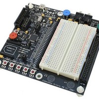
Manufacturer Part Number
EA-EDU-010
Description
MCU, MPU & DSP Development Tools LPC2138 EDUCATION BRD
Manufacturer
Embedded Artists
Specifications of EA-EDU-010
Processor To Be Evaluated
LPC2138
Data Bus Width
16 bit, 32 bit
Interface Type
I2C, SPI, UART
Core
ARM7TDMI-S
Dimensions
127 mm x 120 mm
Maximum Operating Temperature
+ 85 C
Operating Supply Voltage
3.3 V
Lead Free Status / RoHS Status
Lead free / RoHS Compliant


NXP Semiconductors
LPC2131_32_34_36_38
Product data sheet
6.18.1 Crystal oscillator
6.18.2 PLL
6.18.3 Reset and wake-up timer
6.18 System control
On-chip integrated oscillator operates with external crystal in range of 1 MHz to 30 MHz
and with external oscillator up to 50 MHz. The oscillator output frequency is called f
the ARM processor clock frequency is referred to as CCLK for purposes of rate equations,
etc. f
Section 6.18.2 “PLL”
The PLL accepts an input clock frequency in the range of 10 MHz to 25 MHz. The input
frequency is multiplied up into the range of 10 MHz to 60 MHz with a Current Controlled
Oscillator (CCO). The multiplier can be an integer value from 1 to 32 (in practice, the
multiplier value cannot be higher than 6 on this family of microcontrollers due to the upper
frequency limit of the CPU). The CCO operates in the range of 156 MHz to 320 MHz, so
there is an additional divider in the loop to keep the CCO within its frequency range while
the PLL is providing the desired output frequency. The output divider may be set to divide
by 2, 4, 8, or 16 to produce the output clock. Since the minimum output divider value is 2,
it is insured that the PLL output has a 50 % duty cycle. The PLL is turned off and
bypassed following a chip reset and may be enabled by software. The program must
configure and activate the PLL, wait for the PLL to Lock, then connect to the PLL as a
clock source. The PLL settling time is 100 μs.
Reset has two sources on the LPC2131/32/34/36/38: the RESET pin and watchdog reset.
The RESET pin is a Schmitt trigger input pin with an additional glitch filter. Assertion of
chip reset by any source starts the wake-up timer (see wake-up timer description below),
causing the internal chip reset to remain asserted until the external reset is de-asserted,
the oscillator is running, a fixed number of clocks have passed, and the on-chip flash
controller has completed its initialization.
When the internal reset is removed, the processor begins executing at address 0, which is
the reset vector. At that point, all of the processor and peripheral registers have been
initialized to predetermined values.
The wake-up timer ensures that the oscillator and other analog functions required for chip
operation are fully functional before the processor is allowed to execute instructions. This
is important at power on, all types of reset, and whenever any of the aforementioned
functions are turned off for any reason. Since the oscillator and other functions are turned
off during Power-down mode, any wake-up of the processor from Power-down mode
makes use of the wake-up timer.
•
•
•
Match register updates are synchronized with pulse outputs to prevent generation of
erroneous pulses. Software must ‘release’ new match values before they can become
effective.
May be used as a standard timer if the PWM mode is not enabled.
A 32-bit Timer/Counter with a programmable 32-bit Prescaler.
osc
and CCLK are the same value unless the PLL is running and connected. Refer to
All information provided in this document is subject to legal disclaimers.
for additional information.
Rev. 5 — 2 February 2011
LPC2131/32/34/36/38
Single-chip 16/32-bit microcontrollers
© NXP B.V. 2011. All rights reserved.
osc
22 of 45
and
Related parts for EA-EDU-010
Image
Part Number
Description
Manufacturer
Datasheet
Request
R

Part Number:
Description:
MCU, MPU & DSP Development Tools LPC2148 EDUCATION BRD
Manufacturer:
Embedded Artists
Datasheet:

Part Number:
Description:
MCU, MPU & DSP Development Tools LPC2103 EDUCATION BRD
Manufacturer:
Embedded Artists
Datasheet:

Part Number:
Description:
MCU, MPU & DSP Development Tools EXPERIMENT EXPANSION BRD
Manufacturer:
Embedded Artists
Datasheet:

Part Number:
Description:
HEATSINK FOR TO-220 BLACK
Manufacturer:
Ohmite
Datasheet:

Part Number:
Description:
HEATSINK FOR TO-220 BLACK
Manufacturer:
Ohmite
Datasheet:

Part Number:
Description:
HEATSINK FOR TO-220 BLACK
Manufacturer:
Ohmite
Datasheet:

Part Number:
Description:
LCD Graphic Display Modules & Accessories Pure Green Backlight For DOG-M Series
Manufacturer:
ELECTRONIC ASSEMBLY
Datasheet:

Part Number:
Description:
LCD Graphic Display Modules & Accessories Grn LED Backlight For DOG-XL Series
Manufacturer:
ELECTRONIC ASSEMBLY
Datasheet:
Part Number:
Description:
LCD Graphic Display Modules & Accessories Green LED Backlight For DOG-L Series
Manufacturer:
ELECTRONIC ASSEMBLY
Datasheet:

Part Number:
Description:
KIT LPC3141 SODIMM 66X48 200POS
Manufacturer:
Embedded Artists
Datasheet:
Part Number:
Description:
KIT LPC3152 SODIMM 66X48 200POS
Manufacturer:
Embedded Artists
Datasheet:
Part Number:
Description:
BOARD OEM W/LPC2478 MCU
Manufacturer:
Embedded Artists
Datasheet:
Part Number:
Description:
KIT LPC3250 259 WITH QVGA
Manufacturer:
Embedded Artists
Datasheet: