EA-EDU-010 Embedded Artists, EA-EDU-010 Datasheet - Page 23
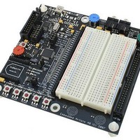
EA-EDU-010
Manufacturer Part Number
EA-EDU-010
Description
MCU, MPU & DSP Development Tools LPC2138 EDUCATION BRD
Manufacturer
Embedded Artists
Specifications of EA-EDU-010
Processor To Be Evaluated
LPC2138
Data Bus Width
16 bit, 32 bit
Interface Type
I2C, SPI, UART
Core
ARM7TDMI-S
Dimensions
127 mm x 120 mm
Maximum Operating Temperature
+ 85 C
Operating Supply Voltage
3.3 V
Lead Free Status / RoHS Status
Lead free / RoHS Compliant


NXP Semiconductors
LPC2131_32_34_36_38
Product data sheet
6.18.4 Brownout detector
6.18.5 Code security
6.18.6 External interrupt inputs
6.18.7 Memory Mapping Control
The wake-up timer monitors the crystal oscillator as the means of checking whether it is
safe to begin code execution. When power is applied to the chip, or some event caused
the chip to exit Power-down mode, some time is required for the oscillator to produce a
signal of sufficient amplitude to drive the clock logic. The amount of time depends on
many factors, including the rate of V
and its electrical characteristics (if a quartz crystal is used), as well as any other external
circuitry (e.g. capacitors), and the characteristics of the oscillator itself under the existing
ambient conditions.
The LPC2131/32/34/36/38 include 2-stage monitoring of the voltage on the V
this voltage falls below 2.9 V, the BOD asserts an interrupt signal to the Vectored Interrupt
Controller. This signal can be enabled for interrupt; if not, software can monitor the signal
by reading dedicated register.
The second stage of low-voltage detection asserts reset to inactivate the
LPC2131/32/34/36/38 when the voltage on the V
prevents alteration of the flash as operation of the various elements of the chip would
otherwise become unreliable due to low voltage. The BOD circuit maintains this reset
down below 1 V, at which point the POR circuitry maintains the overall reset.
Both the 2.9 V and 2.6 V thresholds include some hysteresis. In normal operation, this
hysteresis allows the 2.9 V detection to reliably interrupt, or a regularly-executed event
loop to sense the condition.
Features available only in LPC213x/01 parts include ability to put the BOD in power-down
mode, turn it on or off and to control when the BOD will reset the LPC213x/01
microcontroller. This can be used to further reduce power consumption when a low power
mode (such as Power Down) is invoked.
This feature of the LPC2131/32/34/36/38 allow an application to control whether it can be
debugged or protected from observation.
If after reset on-chip bootloader detects a valid checksum in flash and reads 0x8765 4321
from address 0x1FC in flash, debugging will be disabled and thus the code in flash will be
protected from observation. Once debugging is disabled, it can be enabled only by
performing a full chip erase using the ISP.
The LPC2131/32/34/36/38 include up to nine edge or level sensitive External Interrupt
Inputs as selectable pin functions. When the pins are combined, external events can be
processed as four independent interrupt signals. The External Interrupt Inputs can
optionally be used to wake up the processor from Power-down mode.
The Memory Mapping Control alters the mapping of the interrupt vectors that appear
beginning at address 0x0000 0000. Vectors may be mapped to the bottom of the on-chip
flash memory, or to the on-chip static RAM. This allows code running in different memory
spaces to have control of the interrupts.
All information provided in this document is subject to legal disclaimers.
Rev. 5 — 2 February 2011
DD
ramp (in the case of power on), the type of crystal
LPC2131/32/34/36/38
DD
Single-chip 16/32-bit microcontrollers
pins falls below 2.6 V. This reset
© NXP B.V. 2011. All rights reserved.
DD
pins. If
23 of 45
Related parts for EA-EDU-010
Image
Part Number
Description
Manufacturer
Datasheet
Request
R

Part Number:
Description:
MCU, MPU & DSP Development Tools LPC2148 EDUCATION BRD
Manufacturer:
Embedded Artists
Datasheet:

Part Number:
Description:
MCU, MPU & DSP Development Tools LPC2103 EDUCATION BRD
Manufacturer:
Embedded Artists
Datasheet:

Part Number:
Description:
MCU, MPU & DSP Development Tools EXPERIMENT EXPANSION BRD
Manufacturer:
Embedded Artists
Datasheet:

Part Number:
Description:
HEATSINK FOR TO-220 BLACK
Manufacturer:
Ohmite
Datasheet:

Part Number:
Description:
HEATSINK FOR TO-220 BLACK
Manufacturer:
Ohmite
Datasheet:

Part Number:
Description:
HEATSINK FOR TO-220 BLACK
Manufacturer:
Ohmite
Datasheet:

Part Number:
Description:
LCD Graphic Display Modules & Accessories Pure Green Backlight For DOG-M Series
Manufacturer:
ELECTRONIC ASSEMBLY
Datasheet:

Part Number:
Description:
LCD Graphic Display Modules & Accessories Grn LED Backlight For DOG-XL Series
Manufacturer:
ELECTRONIC ASSEMBLY
Datasheet:
Part Number:
Description:
LCD Graphic Display Modules & Accessories Green LED Backlight For DOG-L Series
Manufacturer:
ELECTRONIC ASSEMBLY
Datasheet:

Part Number:
Description:
KIT LPC3141 SODIMM 66X48 200POS
Manufacturer:
Embedded Artists
Datasheet:
Part Number:
Description:
KIT LPC3152 SODIMM 66X48 200POS
Manufacturer:
Embedded Artists
Datasheet:
Part Number:
Description:
BOARD OEM W/LPC2478 MCU
Manufacturer:
Embedded Artists
Datasheet:
Part Number:
Description:
KIT LPC3250 259 WITH QVGA
Manufacturer:
Embedded Artists
Datasheet: