A2F-DEV-KIT Actel, A2F-DEV-KIT Datasheet - Page 3
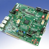
A2F-DEV-KIT
Manufacturer Part Number
A2F-DEV-KIT
Description
MCU, MPU & DSP Development Tools SmartFusion Development Kit
Manufacturer
Actel
Datasheet
1.A2F-DEV-KIT.pdf
(12 pages)
Specifications of A2F-DEV-KIT
Processor To Be Evaluated
A2F200M3F-FGG484
Data Bus Width
32 bit
Interface Type
RS-232, RS-485, Ethernet, USB, I2C, JTAG, SPI
Operating Supply Voltage
5 V
Lead Free Status / RoHS Status
Lead free / RoHS Compliant


SmartFusion Architecture
Along with microcontroller (MCU), FPGA and analog, SmartFusion intelligent mixed signal FPGAs integrate substantial fl ash and SRAM memory
and comprehensive clock generation and management circuitry. SmartFusion architecture enables data storage and execution of code from a
single monolithic device. In addition, in-application programming (IAP) enables real-time updates and reprogramming of the complete chip. Design
compromises that were inevitable with traditional fi xed-function microcontrollers and FPGAs are eliminated when designing with SmartFusion devices.
•
•
•
•
•
•
•
•
Hardware industry-standard 100 MHz,
32-bit ARM Cortex-M3 CPU
Multi-layer AHB communication matrix with
up to 16 Gbps throughput
10/100 Ethernet MAC with RMII interface
Two of each: SPI, I 2 C, UART,
32-bit timers
Up to 512 KB fl ash and 64 KB of SRAM
External memory controller (EMC)
8-channel DMA controller
Up to 41 MSS I/Os with Schmitt
trigger inputs
— 25 I/Os can be used as FPGA I/Os
UART 1
Temp.
Temp.
SPI 1
I 2 C 1
Mon.
Mon.
Mon.
Mon.
Curr.
Curr.
WDT
PLL
MICROCONTROLLER
SUBSYSTEM (MSS)
SCB
SCB
NO-COMPROMISE
Comparator
Comparator
Volt Mon.
Volt Mon.
Supervisor
(ABPS)
(ABPS)
32 KHz
OSC
EFROM
APB
IAP
RTC
RC
ADC
ADC
+
–
3 V
3
PDMA
JTAG
SWD
Analog Compute
Sample Sequencing
Post Processing
ARM
Engine
Engine
Engine
•
•
•
•
•
•
APB
®
High-performance analog signal
conditioning blocks (SCB) with voltage,
current and temperature monitors
Analog compute engine (ACE) offl oads CPU
from analog initialization and processing
of analog-to-digital conversion (ADC),
digital-to-analog conversion (DAC) and SCBs
Integrated ADCs and DACs with
1 percent accuracy
12-/10-/8-bit mode ADCs with
500/550/600 Ksps sampling rate
Up to ten 15 ns high-speed comparators
Up to 32 analog inputs and 3 outputs
Cortex
S
NVIC
D
™
-M3
SysTick
PROGRAMMABLE
EMC
MPU
AHB Bus Matrix
I
ANALOG
(SDD)
(SDD)
DAC
DAC
10/100
EMAC
PPB
SRAM
ESRAM
SysReg
ENVM
SRAM
SRAM
•
•
•
•
Based on Microsemi’s proven
ProASIC3 architecture
60,000 to 500,000 system gates
with 350 MHz system performance
Embedded SRAMs and FIFOs
Up to 128 FPGA I/Os supporting LVDS,
PCI, PCI-X and LVTTL/LVCMOS standards
— Variable aspect ratio 4,608-bit
— x1, x2, x4, x9 and x18 organizations
— True dual-port SRAM (including x18)
SRAM blocks
VersaTiles
........
........
Microcontroller Subsystem
Programmable Analog
FPGA Fabric
NO COMPROMISE
Timer1
Timer2
FPGA FABRIC
APB
SRAM
SRAM
SRAM
UART 2
SPI 2
I 2 C 2
3
Related parts for A2F-DEV-KIT
Image
Part Number
Description
Manufacturer
Datasheet
Request
R

Part Number:
Description:
MCU, MPU & DSP Development Tools Smart Fusion Eval Kit
Manufacturer:
Actel
Datasheet:

Part Number:
Description:
MCU, MPU & DSP Development Tools SmartFusion Motor Control Dev Kit
Manufacturer:
Actel

Part Number:
Description:
MCU, MPU & DSP Development Tools Silicon Sculptor Programming Mod
Manufacturer:
Actel
Part Number:
Description:
MCU, MPU & DSP Development Tools InSystem Programming ProASICPLUS Devices
Manufacturer:
Actel
Part Number:
Description:
Programming Socket Adapters & Emulators PQ160 Module
Manufacturer:
Actel
Part Number:
Description:
Programming Socket Adapters & Emulators Axcelerator Adap Module Kit
Manufacturer:
Actel
Part Number:
Description:
Programming Socket Adapters & Emulators Evaluation
Manufacturer:
Actel
Part Number:
Description:
Programming Socket Adapters & Emulators AFDX Solutions
Manufacturer:
Actel
Part Number:
Description:
Programming Socket Adapters & Emulators SILICON SCULPTOR ADAPTER MODULE
Manufacturer:
Actel
Datasheet:
Part Number:
Description:
Programming Socket Adapters & Emulators Axcelerator Adap Module Kit
Manufacturer:
Actel
Part Number:
Description:
Programming Socket Adapters & Emulators Evaluation
Manufacturer:
Actel
Part Number:
Description:
Programming Socket Adapters & Emulators Silicon Sculptor Software
Manufacturer:
Actel
Part Number:
Description:
Programming Socket Adapters & Emulators InSystem Programming ProASICPLUS Devices
Manufacturer:
Actel
Part Number:
Description:
Programming Socket Adapters & Emulators Evaluation
Manufacturer:
Actel