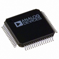
AD7656BSTZ-1 Analog Devices Inc, AD7656BSTZ-1 Datasheet - Page 10

AD7656BSTZ-1
Manufacturer Part Number
AD7656BSTZ-1
Description
6-CHANNEL 16-BIT SE BIPOLAR I.C.
Manufacturer
Analog Devices Inc
Specifications of AD7656BSTZ-1
Number Of Bits
16
Sampling Rate (per Second)
250k
Data Interface
Serial, Parallel
Number Of Converters
6
Power Dissipation (max)
143mW
Voltage Supply Source
Analog and Digital, Dual ±
Operating Temperature
-40°C ~ 85°C
Mounting Type
Surface Mount
Package / Case
64-LQFP
Lead Free Status / RoHS Status
Lead free / RoHS Compliant
For Use With
EVAL-AD7656-1EDZ - BOARD EVAL CONTROL AD7656-1EVAL-AD7656-1CBZ - BOARD EVAL FOR AD7656-1EVAL-AD7656CBZ - BOARD EVAL FOR AD7656
Lead Free Status / RoHS Status
Lead free / RoHS Compliant
Available stocks
Company
Part Number
Manufacturer
Quantity
Price
Company:
Part Number:
AD7656BSTZ-1
Manufacturer:
ADI
Quantity:
3
Company:
Part Number:
AD7656BSTZ-1
Manufacturer:
Analog Devices Inc
Quantity:
10 000
Part Number:
AD7656BSTZ-1
Manufacturer:
ADI/亚德诺
Quantity:
20 000
Company:
Part Number:
AD7656BSTZ-1-RL
Manufacturer:
Analog Devices Inc
Quantity:
10 000
AD7656-1/AD7657-1/AD7658-1
ABSOLUTE MAXIMUM RATINGS
T
Table 5.
Parameter
V
V
V
AV
DV
DV
AGND to DGND
V
Analog Input Voltage to AGND
Digital Input Voltage to DGND
Digital Output Voltage to DGND
REFIN/REFOUT to AGND
Input Current to Any Pin Except
Operating Temperature Range
Storage Temperature Range
Junction Temperature
Pb/Sn Temperature, Soldering
Pb-Free Temperature, Soldering Reflow
ESD
1
2
If the analog inputs are driven from alternative V
a 240 Ω series resistor should be placed on the analog inputs and Schottky
diodes should be placed in series with the AD7656-1/AD7657-1/AD7658-1’s
V
Transient currents of up to 100 mA do not cause SCR latch-up.
DD
SS
DD
DRIVE
A
DD
Supplies
B Version
Y Version
Reflow (10 sec to 30 sec)
CC
CC
CC
= 25°C, unless otherwise noted.
to AGND, DGND
to AGND, DGND
to AV
and V
to AGND, DGND
to AV
to DGND, AGND
to DGND
SS
CC
CC
supplies.
2
1
DD
Rating
−0.3 V to +16.5 V
+0.3 V to −16.5 V
V
−0.3 V to +7 V
−0.3 V to AV
−0.3 V to +7 V
−0.3 V to +0.3 V
−0.3 V to DV
V
−0.3 V to V
−0.3 V to V
−0.3 V to AV
±10 mA
−40°C to +85°C
−40°C to +125°C
−65°C to +150°C
150°C
240(+0)°C
260(+0)°C
700 V
CC
SS
and V
− 0.3 V to V
− 0.3 V to 16.5 V
SS
supply circuitry,
DRIVE
DRIVE
CC
CC
CC
DD
+ 0.3 V
+ 0.3 V
+ 0.3 V
+ 0.3 V
+ 0.3 V
+ 0.3 V
Rev. 0 | Page 10 of 32
Stresses above those listed under Absolute Maximum Ratings
may cause permanent damage to the device. This is a stress
rating only; functional operation of the device at these or any
other conditions above those indicated in the operational
section of this specification is not implied. Exposure to absolute
maximum rating conditions for extended periods may affect
device reliability.
THERMAL RESISTANCE
θ
soldered in a circuit board for surface-mount packages. These
specifications apply to a 4-layer board.
Table 6. Thermal Resistance
Package Type
64-Lead LQFP
ESD CAUTION
JA
is specified for the worst-case conditions, that is, a device
θ
45
JA
θ
11
JC
Unit
°C/W


