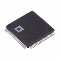
AD9980KSTZ-80 Analog Devices Inc, AD9980KSTZ-80 Datasheet - Page 19

AD9980KSTZ-80
Manufacturer Part Number
AD9980KSTZ-80
Description
IC,Data Acquisition Signal Conditioner,3-CHANNEL,8-BIT,CMOS,QFP,80PIN,PLASTIC
Manufacturer
Analog Devices Inc
Datasheet
1.AD9980KSTZ-80.pdf
(44 pages)
Specifications of AD9980KSTZ-80
Applications
Video
Interface
Analog
Voltage - Supply
3.13 V ~ 3.47 V
Package / Case
80-LQFP
Mounting Type
Surface Mount
Lead Free Status / RoHS Status
Lead free / RoHS Compliant
For Use With
AD9980/PCBZ - KIT EVALUATION AD9980
Lead Free Status / RoHS Status
Lead free / RoHS Compliant
Available stocks
Company
Part Number
Manufacturer
Quantity
Price
Company:
Part Number:
AD9980KSTZ-80
Manufacturer:
ADI
Quantity:
830
Company:
Part Number:
AD9980KSTZ-80
Manufacturer:
Analog Devices Inc
Quantity:
10 000
Part Number:
AD9980KSTZ-80
Manufacturer:
ADI/亚德诺
Quantity:
20 000
TIMING DIAGRAMS
The following timing diagrams show the operation of the
AD9980.The output data clock signal is created so that its rising
edge always occurs between data transitions and can be used to
CB/CROUT
DATAOUT
DATACLK
DATACLK
DATAIN
DATAIN
HSOUT
HSOUT
YOUT
HSIN
HSIN
1. PIXEL AFTER HSOUT CORRESONDS TO BLUE INPUT.
2. EVEN NUMBER OF PIXEL DELAY BETWEEN HSOUT AND DATAOUT (6 FOR THE AD9980).
P0
P0
DATACK
HSOUT
P1
P1
DATA
P2
P2
2 CLOCK CYCLE DELAY
2 CLOCK CYCLE DELAY
P3
P3
t
DCYCLE
–t
Figure 14. 4:4:4 Timing Mode
Figure 15. 4:2:2 Timing Mode
SKEW
Figure 13. Output Timing
+t
P4
P4
SKEW
Rev. 0 | Page 19 of 44
t
PER
P5
P5
P6
P6
latch the output data externally. There is a pipeline in the
AD9980, which must be flushed before valid data becomes
available. This means six data sets are presented before valid
data is available.
P7
P7
P8
8 CLOCK CYCLE DELAY
P8
8 CLOCK CYCLE DELAY
P0
Y0
B0
P9
P9
P1
Y1
R0
P10
P10
P2
Y2
B2
P11
P11
P3
Y3
R2
AD9980


