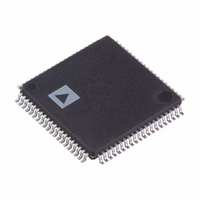
AD9980KSTZ-80 Analog Devices Inc, AD9980KSTZ-80 Datasheet - Page 20

AD9980KSTZ-80
Manufacturer Part Number
AD9980KSTZ-80
Description
IC,Data Acquisition Signal Conditioner,3-CHANNEL,8-BIT,CMOS,QFP,80PIN,PLASTIC
Manufacturer
Analog Devices Inc
Datasheet
1.AD9980KSTZ-80.pdf
(44 pages)
Specifications of AD9980KSTZ-80
Applications
Video
Interface
Analog
Voltage - Supply
3.13 V ~ 3.47 V
Package / Case
80-LQFP
Mounting Type
Surface Mount
Lead Free Status / RoHS Status
Lead free / RoHS Compliant
For Use With
AD9980/PCBZ - KIT EVALUATION AD9980
Lead Free Status / RoHS Status
Lead free / RoHS Compliant
Available stocks
Company
Part Number
Manufacturer
Quantity
Price
Company:
Part Number:
AD9980KSTZ-80
Manufacturer:
ADI
Quantity:
830
Company:
Part Number:
AD9980KSTZ-80
Manufacturer:
Analog Devices Inc
Quantity:
10 000
Part Number:
AD9980KSTZ-80
Manufacturer:
ADI/亚德诺
Quantity:
20 000
AD9980
HSYNC TIMING
The Hsync is processed in the AD9980 to eliminate ambiguity
in the timing of the leading edge with respect to the phase-
delayed pixel clock and data.
The Hsync input is used as a reference to generate the pixel
sampling clock. The sampling phase can be adjusted with
respect to Hsync through a full 360° in 32 steps via the phase
adjust register (to optimize the pixel sampling time). Display
systems use Hsync to align memory and display write cycles, so
it is important to have a stable timing relationship between
Hsync output (HSOUT) and the data clock (DATACK).
Three things happen to Hsync in the AD9980. First, the polarity
of Hsync input is determined and thus has a known output
polarity. The known output polarity can be programmed either
active high or active low (Register 0x12, Bit 3). Second, HSOUT
is aligned with DATACK and data outputs. Third, the duration
of HSOUT (in pixel clocks) is set via Register 0x13. HSOUT is
the sync signal that should be used to drive the rest of the
display system.
COAST TIMING
In most computer systems, the Hsync signal is continuously
provided on a dedicated wire. In these systems, the Coast input
and function are unnecessary and should not be used.
In some systems, however, Hsync is disturbed during Vsync. In
some cases, Hsync pulses disappear. In other systems, such as
those that employ composite sync (Csync) signals or embedded
sync-on-green, Hsync may include equalization pulses or other
distortions during Vsync. To avoid upsetting the clock generator
during Vsync, it is important to ignore these distortions. If the
pixel clock PLL sees extraneous pulses, it attempts to lock to this
new frequency, and will change frequency by the end of the
Vsync period. It then takes a few lines of correct Hsync timing
to recover at the beginning of a new frame, resulting in a tearing
of the image at the top of the display.
DATACLK
DATAIN
HSOUT
HSIN
DDR NOTES
1. OUTPUT DATACLK MAY BE DELAYED 1/4 CLOCK PERIOD IN THE REGISTERS.
2. FOR DDR 4:2:2 MODE: TIMING IS IDENTICAL, VALUES OF F (FALLING EDGE) AND R (RISING EDGE) CHANGE.
GENERAL NOTES
1. DATA DELAY MAY VARY ± ONE CLOCK CYCLE, DEPENDING ON PHASE SETTING.
2. ADCs SAMPLE INPUT ON FALLING EDGE OF DATACLK.
3. HSYNC SHOWN IS ACTIVE HIGH (EDGE SHOWN IS LEADING EDGE).
P0
P1
P2
2 CLOCK CYCLE DELAY
P3
Figure 16. DDR Timing Mode
P4
Rev. 0 | Page 20 of 44
P5
P6
The Coast input is provided to eliminate this problem. It is an
asynchronous input that disables the PLL input and holds the
clock at its current frequency. The PLL can run free for several
lines without significant frequency drift. Coast can be generated
internally by the AD9980 (see Register 0x18) or can be provided
externally by the graphics controller.
When internal Coast is selected (Register 0x18, Bit 7 = 0, and
Register 0x14, Bits [7:6] to select source), the Vsync is used as
the basis for determining the position of Coast. The internal
Coast signal is enabled a programmed number of Hsync
periods before the periodic Vsync signal (Precoast
Register 0x16) and dropped a programmed number of Hsync
periods after the Vsync (Postcoast Register 0x17). It is
recommended that the Vsync filter be enabled when using the
internal Coast function to allow the AD9980 to precisely
determine the number of Hsyncs/Vsync and their location. In
many applications where disruptions occur and Coast is used,
values of 2 for the Precoast and 10 for Postcoast are sufficient to
avoid most extraneous pulses.
OUTPUT FORMATTER
The output formatter is capable of generating several output
formats to be presented to the 24 data output pins. The output
formats and the pin assignments for each format are listed in
Table 11. Also, there are several clock options for the output
clock. The user may select the pixel clock, a 90° phase-shifted
pixel clock, a 2× pixel clock, or a fixed frequency 40 MHz clock
for test purposes. The output clock may also be inverted.
Data output is available as a 24-pin RGB or YCbCr, or if either
4:2:2 or 4:4:4 DDR is selected, a secondary channel is available.
This secondary channel is always 4:2:2 DDR and allows the
flexibility of having a second channel with the same video data
that can be utilized by another display or a storage device.
Depending on the choice of output modes, the primary output
can be 24 pins, 16 pins or as few as 12 pins.
P7
P8
F0 R0 F1 R1 F2 R2 F3 R3
8 CLOCK CYCLE DELAY
P9
Preliminary Technical Data
P10
P11


