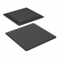
ADSP-21160MKBZ-80 Analog Devices Inc, ADSP-21160MKBZ-80 Datasheet - Page 44

ADSP-21160MKBZ-80
Manufacturer Part Number
ADSP-21160MKBZ-80
Description
32bit SHARC W/SIMD Capability
Manufacturer
Analog Devices Inc
Series
SHARC®r
Type
Floating Pointr
Specifications of ADSP-21160MKBZ-80
Interface
Host Interface, Link Port, Serial Port
Clock Rate
80MHz
Non-volatile Memory
External
On-chip Ram
512kB
Voltage - I/o
3.30V
Voltage - Core
2.50V
Operating Temperature
0°C ~ 85°C
Mounting Type
Surface Mount
Package / Case
400-BGA
Device Core Size
32b
Architecture
Enhanced Harvard
Format
Floating Point
Clock Freq (max)
80MHz
Mips
80
Device Input Clock Speed
80MHz
Ram Size
512KB
Operating Supply Voltage (typ)
2.5/3.3V
Operating Supply Voltage (min)
2.37/3.13V
Operating Supply Voltage (max)
2.63/3.47V
Operating Temp Range
0C to 85C
Operating Temperature Classification
Commercial
Mounting
Surface Mount
Pin Count
400
Package Type
BGA
Lead Free Status / RoHS Status
Lead free / RoHS Compliant
Lead Free Status / RoHS Status
Lead free / RoHS Compliant, Lead free / RoHS Compliant
Available stocks
Company
Part Number
Manufacturer
Quantity
Price
Company:
Part Number:
ADSP-21160MKBZ-80
Manufacturer:
AD
Quantity:
310
Company:
Part Number:
ADSP-21160MKBZ-80
Manufacturer:
Analog Devices Inc
Quantity:
10 000
ADSP-21160M
Example: Estimate P
• A system with one bank of external data memory—asyn-
• Four 64K × 16 RAM chips are used, each with a load of
Table 30. External Power Calculations (3.3 V Device)
these conditions by adding a typical internal power
dissipation:
Where:
• P
• P
• P
Note that the conditions causing a worst-case P
different from those causing a worst-case P
P
switching from all ones to all zeros. Note also that it is not
common for an application to have 100% or even 50% of
the outputs switching simultaneously.
Test Conditions
The test conditions for timing parameters appearing in
ADSP-21160M specifications on page 13
disable time, output enable time, and capacitive loading.
Output Disable Time
Output pins are considered to be disabled when they stop
driving, go into a high impedance state, and start to decay
from their output high or low voltage. The time for the
voltage on the bus to decay by –V is dependent on the capac-
itive load, C
be approximated by the following equation:
The output disable time t
t
is the interval from when the reference signal switches to
when the output voltage decays –V from the measured
output high or output low voltage. t
test loads C
Pin Type
Address
MS0
WRx
Data
CLKOUT
A typical power consumption can now be calculated for
MEASURED
INT
chronous RAM (64-bit)
10 pF
Power Dissipation on page 42
ABSOLUTE MAXIMUM RATINGS on page 14
EXT
INT
PLL
cannot occur while 100% of the output pins are
is I
is AI
is from
and t
DDINT
DD
L
L
and I
DECAY
and the load current, I
× 2.5V, using the value for AI
× 2.5V, using the calculation I
Table 30
# of Pins
15
1
2
64
1
P
as shown in
L
, and with –V equal to 0.5 V.
TOTAL
t
EXT
DECAY
= P
with the following assumptions:
DIS
= (C
EXT
is the difference between
Figure
+ P
L
INT
V)/I
% Switching
50
0
–
50
–
DECAY
L
. This decay time can
30. The time t
+ P
L
is calculated with
PLL
include output
INT
DD
DDINT
. Maximum
listed in
EXT
listed in
are
MEASURED
× C
× 44.7 pF
× 44.7 pF
× 44.7 pF
× 14.7 pF
× 4.7 pF
–44–
• External data memory writes occur every other cycle, a
• The bus cycle time is 40 MHz (t
The P
can drive:
Output Enable Time
Output pins are considered to be enabled when they have
made a transition from a high impedance state to when they
start driving. The output enable time t
when a reference signal reaches a high or low voltage level
to when the output has reached a specified high or low trip
point, as shown in the Output Enable/Disable diagram
(Figure
enabled, the measurement value is that of the first pin to
start driving.
Example System Hold Time Calculation
To determine the data output hold time in a particular
system, first calculate t
Choose –V to be the difference between the
ADSP-21160M’s output voltage and the input threshold for
the device requiring the hold time. A typical –V will be 0.4 V.
C
total leakage or three-state current (per data line). The hold
time will be t
t
Figure 30. Output Enable/Disable
DATRWH
L
rate of 1/(4 t
is the total bus capacitance (per data line), and I
V OL (MEASURED)
V OH (MEASURED)
EXT
RE F E R E NCE
× f
× 12.5 MHz
× 12.5 MHz
× 25 MHz
× 12.5 MHz
× 25 MHz
for the write cycle).
30). If multiple pins (such as the data bus) are
S IG NA L
equation is calculated for each class of pins that
DECAY
CK
t
), with 50% of the pins switching
DIS
plus the minimum disable time (i.e.,
O UT P UT S T O PS
DR IV IN G
DECAY
× VDD
× 10.9 V
× 10.9 V
× 10.9 V
× 10.9 V
× 10.9 V
T E S T CO ND ITIO N S CA US E T HIS V O L T AG E
t
MEASURED
using the equation given above.
V OL (MEASURED) + D V
V OH (MEASURED) – D V
t
DECAY
T O BE A PP R O X IM A TE L Y 1.5V
HIG H -IM P E D AN CE S T AT E .
2
CK
= 25 ns).
ENA
is the interval from
= P
= 0.046 W
= 0.000 W
= 0.024 W
= 0.064 W
= 0.001 W
P
O UT P UT S T AR T S
EXT
t
1.0V
ENA
2.0V
EXT
DR IV IN G
= 0.135 W
L
REV. 0
is the


