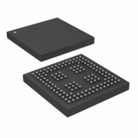
ADSP-21262SBBCZ150 Analog Devices Inc, ADSP-21262SBBCZ150 Datasheet - Page 14

ADSP-21262SBBCZ150
Manufacturer Part Number
ADSP-21262SBBCZ150
Description
IC,DSP,32-BIT,CMOS,BGA,136PIN,PLASTIC
Manufacturer
Analog Devices Inc
Series
SHARC®r
Type
Fixed/Floating Pointr
Specifications of ADSP-21262SBBCZ150
Interface
DAI, SPI
Clock Rate
150MHz
Non-volatile Memory
ROM (512 kB)
On-chip Ram
256kB
Voltage - I/o
3.30V
Voltage - Core
1.20V
Operating Temperature
-40°C ~ 85°C
Mounting Type
Surface Mount
Package / Case
136-CSPBGA
Device Core Size
32/40Bit
Architecture
Super Harvard
Format
Floating Point
Clock Freq (max)
150MHz
Mips
150
Device Input Clock Speed
150MHz
Ram Size
256KB
Program Memory Size
512KB
Operating Supply Voltage (typ)
1.2/3.3V
Operating Supply Voltage (min)
1.14/3.13V
Operating Supply Voltage (max)
1.26/3.47V
Operating Temp Range
0C to 70C
Operating Temperature Classification
Commercial
Mounting
Surface Mount
Pin Count
136
Package Type
CSPBGA
Package
136CSP-BGA
Numeric And Arithmetic Format
Floating-Point
Maximum Speed
150 MHz
Device Million Instructions Per Second
150 MIPS
Lead Free Status / RoHS Status
Lead free / RoHS Compliant
Lead Free Status / RoHS Status
Lead free / RoHS Compliant
Available stocks
Company
Part Number
Manufacturer
Quantity
Price
Company:
Part Number:
ADSP-21262SBBCZ150
Manufacturer:
Analog Devices Inc
Quantity:
10 000
Part Number:
ADSP-21262SBBCZ150
Manufacturer:
ADI/亚德诺
Quantity:
20 000
ADSP-21262
ADDRESS DATA PINS AS FLAGS
To use these pins as flags (FLAG15–0) set (=1) Bit 20 of the
SYSCTL register and disable the parallel port.
Table 3. AD15–0 to FLAG Pin Mapping
Boot Modes
Table 4. Boot Mode Selection
CORE INSTRUCTION RATE TO CLKIN RATIO MODES
Table 5. Core Instruction Rate/CLKIN Ratio Selection
AD Pin
AD0
AD1
AD2
AD3
AD4
AD5
AD6
AD7
AD8
AD9
AD10
AD11
AD12
AD13
AD14
AD15
BOOTCFG1–0
00
01
10
11
CLKCFG1–0
00
01
10
11
Flag Pin
FLAG8
FLAG9
FLAG10
FLAG11
FLAG12
FLAG13
FLAG14
FLAG15
FLAG0
FLAG1
FLAG2
FLAG3
FLAG4
FLAG5
FLAG6
FLAG7
Booting Mode
SPI Slave Boot
SPI Master Boot
Parallel Port Boot via EPROM
Internal Boot Mode (ROM code only)
Core to CLKIN Ratio
3:1
16:1
8:1
Reserved
Rev. B | Page 14 of 48 | August 2005
ADDRESS DATA MODES
Table 6
16-bit transfers to the parallel port. For 8-bit data transfers, ALE
latches address bits A23–A8 when asserted, followed by address
bits A7–A0 and data bits D7–D0 when deasserted. For 16-bit
data transfers, ALE latches address bits A15–A0 when asserted,
followed by data bits D15–D0 when deasserted.
Table 6. Address/Data Mode Selection
EP Data
Mode
8-bit
8-bit
16-bit
16-bit
shows the functionality of the AD pins for 8-bit and
ALE
Asserted
Deasserted
Asserted
Deasserted
AD7–0
Function
A15–8
D7–0
A7–0
D7–0
AD15–8
Function
A23–16
A7–0
A15–8
D15–8


