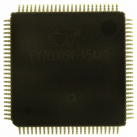
CY7C009V-15AXC Cypress Semiconductor Corp, CY7C009V-15AXC Datasheet - Page 9

CY7C009V-15AXC
Manufacturer Part Number
CY7C009V-15AXC
Description
CY7C009V-15AXC
Manufacturer
Cypress Semiconductor Corp
Datasheet
1.CY7C009V-15AXC.pdf
(23 pages)
Specifications of CY7C009V-15AXC
Format - Memory
RAM
Memory Type
SRAM - Dual Port, Asynchronous
Memory Size
1M (128K x 8)
Speed
15ns
Interface
Parallel
Voltage - Supply
3 V ~ 3.6 V
Operating Temperature
0°C ~ 70°C
Package / Case
100-LQFP
Lead Free Status / RoHS Status
Lead free / RoHS Compliant
Other names
428-1786
Available stocks
Company
Part Number
Manufacturer
Quantity
Price
Company:
Part Number:
CY7C009V-15AXC
Manufacturer:
CYPRESS
Quantity:
233
Company:
Part Number:
CY7C009V-15AXC
Manufacturer:
Cypress Semiconductor Corp
Quantity:
10 000
Part Number:
CY7C009V-15AXC
Manufacturer:
CYPRESS/赛普拉斯
Quantity:
20 000
Switching Characteristics
Over the Operating Range
Document Number: 38-06044 Rev. *E
t
t
t
t
t
t
t
t
t
t
t
t
t
t
t
t
t
t
t
t
t
t
t
t
t
t
Notes
WC
SCE
AW
HA
SA
PWE
SD
HD
HZWE
LZWE
WDD
DDD
BLA
BHA
BLC
BHC
PS
WB
WH
BDD
INS
INR
SOP
SWRD
SPS
SAA
16. To access RAM, CE = L, UB = L, SEM = H. To access semaphore, CE = H and SEM = L. Either condition must be valid for the entire t
17. Test conditions used are Load 2.
18. This parameter is guaranteed by design, but it is not production tested.For information on port-to-port delay through RAM cells from writing port to reading port,
19. For information on port-to-port delay through RAM cells from writing port to reading port, refer to Read Timing with Busy waveform.
20. Test conditions used are Load 1.
21. t
WRITE CYCLE
BUSY TIMING
INTERRUPT TIMING
SEMAPHORE TIMING
Parameter
[16]
refer to Read Timing with Busy waveform.
BDD
[16]
[21]
[19]
[19]
[17, 18]
[17, 18]
is a calculated parameter and is the greater of t
[20]
Write cycle time
CE LOW to write end
Address valid to write end
Address hold from write end
Address set-up to write start
Write pulse width
Data set-up to write end
Data hold from write end
R/W LOW to high Z
R/W HIGH to low Z
Write pulse to data delay
Write data valid to read data valid
BUSY LOW from address match
BUSY HIGH from address mismatch
BUSY LOW from CE LOW
BUSY HIGH from CE HIGH
Port set-up for priority
R/W HIGH after BUSY (Slave)
R/W HIGH after BUSY HIGH (Slave)
BUSY HIGH to data valid
INT set time
INT reset time
SEM flag update pulse (OE or SEM)
SEM flag write to read time
SEM flag contention window
SEM address access time
[20]
[11]
(continued)
Description
WDD
–t
PWE
(actual) or t
DDD
Min
15
12
12
12
10
13
10
0
0
0
–
3
–
–
–
–
–
–
5
0
–
–
–
5
5
–
–t
SD
–15
(actual).
Max
10
30
25
15
15
15
15
15
15
15
15
–
–
–
–
–
–
–
–
–
–
–
–
–
–
–
CY7C018V/019V
Min
20
16
16
17
12
15
10
0
0
0
–
3
–
–
–
–
–
–
5
0
–
–
–
5
5
–
–20
Max
12
40
30
20
20
20
16
20
20
20
20
–
–
–
–
–
–
–
–
–
–
–
–
–
–
–
Min
20
20
15
25
22
17
12
0
0
–
3
–
–
–
–
–
–
5
0
–
–
–
5
5
–
0
CY7C008V/009V
CY7C018V/019V
–25
SCE
Max
15
35
20
20
20
17
25
20
20
25
time.
50
–
–
–
–
–
–
–
–
–
–
–
–
–
–
–
Page 9 of 23
Unit
ns
ns
ns
ns
ns
ns
ns
ns
ns
ns
ns
ns
ns
ns
ns
ns
ns
ns
ns
ns
ns
ns
ns
ns
ns
ns
[+] Feedback


